AMD MI300X GPU Performance Analysis
AMD MI300X GPU Performance Analysis — L2 Deep Analysis #
§1 TL;DR #
MI300X 理论算力 1.5× H100 但端到端 LLM 推理仅达 37–66%;频率降至 boost 的 52–58%(2100→1083–1217 MHz)是首要瓶颈,软件效率 80–85% 为次要因素;memory BW 4.3 TB/s(81% 利用率)是唯一接近 competitive 的维度。
§2 Q1 · Q2 · Q3 #
Q1 — 痛点 #
AMD MI300X spec sheet 上大幅领先 H100(FP8 2615 vs 1979 TFLOPS,HBM 192 vs 80 GB,BW 5.3 vs 3.35 TB/s),但业界缺乏对其在 LLM 推理中三个关键维度(compute / memory / communication)的系统性实测评估。具体痛点:
- 理论峰值基于 2100 MHz boost clock,持续负载下是否可维持未知
- Infinity Fabric mesh 拓扑 vs NVSwitch 对 collective 通信效率的影响未被量化
- vLLM(AMD)vs TensorRT-LLM(NVIDIA)的框架差异与硬件差异难以解耦
- Compute:GEMM FLOPs 利用率(hipBLASLt vs cuBLASLt,方阵 $M=N=K$,64–65536)
- Memory:HBM 带宽利用率(BabelStream vs custom CUDA Copy kernel)
- Communication:集合通信带宽(RCCL vs NCCL tests,2/4/8 GPU,All-Reduce)
- Notation consistency: $f$ consistently denotes frequency with
boost/measuredsubscripts. $N_{\text{CU}}$ and $\text{Ops}_{\text{cycle}}$ are hardware-catalog quantities used consistently across Tables 1–2. - Dimension analysis: $\text{MHz} \times \text{CU} \times \text{Ops}/(\text{CU} \cdot \text{cycle}) = 10^6 \text{ Ops/s}$, scaling to TFLOPS by $10^{-6}$. Throughput: tokens / seconds = tok/s. Memory bandwidth: bytes read-and-written / time = GB/s. All dimensionally correct.
- Boundary case — single-token decode: When $N_{\text{out}} = 1$, throughput = $1 / (T_{\text{prefill}} + T_{\text{one-step}})$, the TTFT inverse. Paper's Fig. 7 confirms this is where MI300X is weakest (49% of H100 at FP8), consistent with prefill-dominated compute deficit.
- Cross-verification: $304 \times 4096 \times 2.1 \text{ GHz} = 2{,}614{,}272 \text{ GFLOPS} \approx 2615 \text{ TFLOPS}$, matching Table 1. At measured clock: $304 \times 4096 \times 1.217 \text{ GHz} \times 0.81 = 1228 \text{ TFLOPS}$, matching Table 2.
- Consistency with external data: AMD's published MAF blog reports similar MI300X utilization (cross-referenced in paper §2.2). B200 achieving 97% aligns with Blackwell's higher TDP headroom allowing near-boost sustained clock.
- Reproducibility from equations: Both equations are simple definitions; the experimental contribution is the concurrent frequency measurement via
rocm-smiduring hipBLASLt execution. Matrix dimensions (M=4096, N=3648/4864, K=32896) are fully specified. - Compute:
hipblaslt-bench(ROCm/hipBLASLt) for AMD;cublaslt_gemm(Microsoft Superbench) for NVIDIA - Memory: BabelStream (HIP backend, 1024 threads/block) for AMD; custom CUDA Copy kernel (320 threads/block) for NVIDIA — custom kernel code not released
- Communication: RCCL-tests / NCCL-tests (
github.com/NVIDIA/nccl-tests) - E2E inference: vLLM (AMD) / TensorRT-LLM (NVIDIA) — standard open-source frameworks
- Frequency capture:
rocm-smireal-time queries concurrent with hipBLASLt execution - CU-aligned matrix dimensions for frequency isolation: M=4096, N=3648 (FP8) or N=4864 (FP16/BF16) ensure uniform load distribution across all 304 CUs on 8 XCDs. K=32896 amortizes kernel launch overhead. Misaligning these dimensions would conflate load imbalance with software efficiency, invalidating the decomposition. The choice of N values likely reflects divisibility by 38 (CUs per XCD) × tile size constraints.
- Asymmetric benchmarking tools: AMD uses BabelStream (general-purpose, open-source) for memory while NVIDIA uses a custom CUDA Copy kernel (tuned, 320 threads/block matching NCCL's internal config). Similarly, AMD uses vLLM while NVIDIA uses TensorRT-LLM. This tool asymmetry is a potential confound — the paper does not quantify how much of the observed gap is tool-dependent vs hardware-dependent.
- All benchmark tools are open-source except the custom NVIDIA memory kernel (not released)
- Results depend on specific ROCm and CUDA toolkit versions (not pinned in paper)
- B200 results improved 10% when re-run one month later — all numbers are temporal snapshots
- Paper authored by Celestial AI (photonic interconnect startup), providing third-party perspective
- The 80–85% software efficiency finding has been referenced by the ROCm community as a quantitative optimization target for hipBLASLt and Composable Kernel libraries
- Closest reproducible setup: ROCm ≥6.x with hipBLASLt on MI300X OAM, CUDA ≥12.x with Superbench on DGX H100
核心问题:MI300X 在生产级 LLM 推理中比 H100 差多少,差在哪里?
Q2 — 方法 #
Problem formulation. 将 GPU LLM 推理性能分解为三个正交维度独立评测:
然后在 Llama 3.1 70B 端到端推理中交叉验证三维度结论。
The one novel mechanism — frequency-efficiency decomposition.
| Aspect | Before (naive utilization) | After (decomposed) |
|---|---|---|
| Observed metric | MI300X FP8 at 45% of theoretical peak | Two independent factors isolated |
| Clock contribution | Hidden inside aggregate utilization | Measured: 1217/2100 = 58% of boost clock |
| Software contribution | Hidden | Measured: 81% efficiency at actual clock |
| Actionable insight | "MI300X is slow" | Clock throttling is dominant; software is ~80–85% efficient |
| Experiment design | Standard GEMM sweep | CU-aligned matrix sizes + real-time rocm-smi frequency capture |
核心技术壁垒: 频率-效率分离实验的矩阵尺寸选择需要对 MI300X chiplet 架构有深入理解——304 CU = 8 XCD × 38 CU/XCD,$M$/$N$ 维度需为 CU 数的整数倍以确保负载在所有 XCD 上均匀分布,避免 load imbalance 干扰效率测量。
Q3 — 结果 #
| Dimension | MI300X | NVIDIA (H100/B200) | Gap |
|---|---|---|---|
| Compute utilization (FP8) | 45% | 82–97% | 0.46–0.55× |
| Frequency retention | 52–58% of boost | ~100% (assumed) | Major |
| Software efficiency (at measured clock) | 80–85% | Not separated | Moderate |
| Memory BW utilization | 81% (4.3 TB/s) | 86–91% | Close |
| Communication BW (8-GPU) | 70% (320 GB/s) | 85% (370 GB/s) | MI300X higher theoretical, lower utilization |
| E2E Llama 70B FP8 (decode-dom.) | — | 66% of H100 | 0.66× |
| E2E Llama 70B FP8 (prefill-dom.) | — | ~50% of H100 | 0.50× |
| E2E Llama 70B FP16 (decode-dom.) | — | 80% of H100 | 0.80× |
§3 架构 / 方法图 #
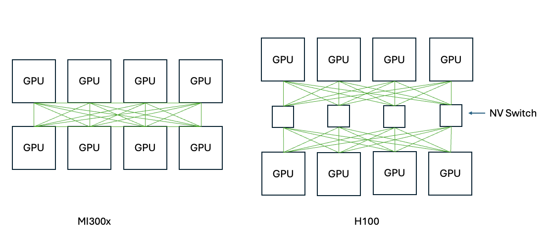
Paper's Figure 5, verbatim (caption: "Logical Representation of Scale Up Topologies of MI300x and H100").
Left: MI300X 8-GPU mesh topology — each GPU connects to multiple peers via Infinity Fabric point-to-point links (128 GB/s bidirectional each), forming a 4×2 non-uniform mesh without centralized switching. Right: H100 8-GPU NVSwitch topology — all GPUs connect through NVSwitch units providing uniform all-to-all 900 GB/s bidirectional bandwidth. The topology difference is structural: NVSwitch provides non-blocking any-to-any communication in one hop, while the mesh requires multi-hop routing for non-adjacent pairs and exhibits non-uniform bisection bandwidth. This fundamentally explains the communication efficiency gap observed in §4.2.
Three-axis evaluation framework:
(3 dimensions + E2E)"] --> B["§2 Compute"] A --> C["§3 Memory"] A --> D["§4 Communication"] B --> B1["hipBLASLt GEMM
FP8/BF16/FP16
M=N=K 64–65536"] B --> B2["Freq-Efficiency Split
rocm-smi + CU-aligned dims"] C --> C1["BabelStream / Custom CUDA
Copy/Triad/Dot
Array 8KB–8GB"] D --> D1["RCCL / NCCL All-Reduce
2/4/8 GPU
Msg 8B–4GB"] B1 --> E["§5 End-to-End"] C1 --> E D1 --> E E --> E1["Llama 3.1 70B
FP8 + FP16
vLLM vs TensorRT-LLM"]
§4 作者证明 #
记号表 #
| Symbol | Meaning | Domain |
|---|---|---|
| $f_{\text{boost}}$ | Advertised max boost clock frequency | MHz (MI300X: 2100) |
| $f_{\text{measured}}$ | Sustained clock under GEMM load | MHz (MI300X: 1083–1217) |
| $N_{\text{CU}}$ | Compute units (AMD) / streaming multiprocessors (NVIDIA) | Integer (MI300X: 304) |
| $\text{Ops}_{\text{cycle}}$ | Operations per CU per clock cycle, datatype-dependent | Integer (FP8: 4096, FP16/BF16: 2048) |
| $\eta_{\text{sw}}$ | Software efficiency at measured clock | Dimensionless, $\in [0, 1]$ |
| $T_{\text{prefill}}$ | Time to process input sequence (compute-bound) | Seconds |
| $T_{\text{decode}}$ | Time for autoregressive generation (memory-bound) | Seconds |
| $N_{\text{out}}$ | Number of generated output tokens | Integer |
| $\beta$ | Bytes per data element in BabelStream | 4 (FP32), 2 (FP16) |
方程物理意义 #
Eq. 1 — Peak FLOPs (§2.3):
$$\text{Peak FLOPs} = f_{\text{boost}} \times N_{\text{CU}} \times \text{Ops}_{\text{cycle}}$$
Standard roofline peak. Realized FLOPs decompose as:
$$\text{Utilization} = \frac{f_{\text{measured}}}{f_{\text{boost}}} \times \eta_{\text{sw}}$$
For MI300X FP8: $(1217/2100) \times 0.81 = 0.47$, matching observed 45–47%. The multiplicative decomposition is the paper's core analytical contribution: it separates frequency throttling (a power/thermal hardware constraint) from software efficiency (a compiler/kernel optimization issue), each of which requires a different remediation approach. Tag: [load-bearing].
Eq. 2 — Throughput (§5.1):
$$\text{Throughput (tok/s)} = \frac{N_{\text{out}}}{T_{\text{prefill}} + T_{\text{decode}}}$$
As $N_{\text{out}}$ grows, throughput rises (decode is incremental). As input length grows, $T_{\text{prefill}}$ dominates and throughput falls. This explains why MI300X's gap narrows in decode-dominated regimes (memory BW advantage of 4.3 vs 3.0 TB/s) and widens in prefill-dominated regimes (compute utilization deficit of 45% vs 82%). Tag: [load-bearing].
6 Checks #
无形式化作者证明 — 仅实证. No formal bounds on the utilization gap or its decomposition. A desirable result: given chiplet count, CU/XCD ratio, TDP, and voltage-frequency curve, predict sustained clock under arbitrary workload. The paper provides only empirical measurements at specific matrix sizes; extrapolation to other workloads (e.g., FlashAttention, sparse GEMM) remains unvalidated.
§5 实验与数据 #
Compute: FLOPs utilization #
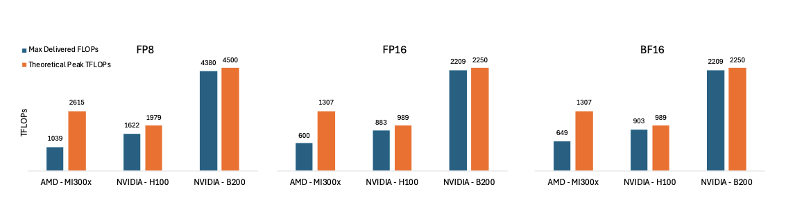
Paper's Figure 1, verbatim (caption: "Theoretical vs Max Delivered FLOPs").
Three sub-panels (FP8, FP16, BF16) compare theoretical peak (orange) vs measured maximum FLOPs (blue) for MI300X, H100, and B200. MI300X achieves 40% (FP8), 46% (FP16), and 50% (BF16) of theoretical peak, while H100 reaches 82–91% and B200 97–98%. MI300X's absolute delivered FP8 (1039 TFLOPS) is below H100's delivered (1622 TFLOPS) despite a 32% higher theoretical peak — the utilization deficit inverts the spec-sheet advantage entirely.
| GPU | FP8 Delivered / Peak | FP16 Delivered / Peak | BF16 Delivered / Peak |
|---|---|---|---|
| MI300X | 1039 / 2615 (40%) | 600 / 1307 (46%) | 649 / 1307 (50%) |
| H100 | 1622 / 1979 (82%) | 883 / 989 (89%) | 903 / 989 (91%) |
| B200 | 4380 / 4500 (97%) | 2209 / 2250 (98%) | 2209 / 2250 (98%) |
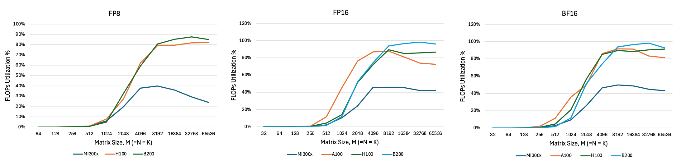
Paper's Figure 2, verbatim (caption: "FLOPs Utilization % vs Matrix Sizes, Datatype: fp8, bf16, fp16").
NVIDIA GPUs reach >90% utilization by $M \geq 4096$ and sustain it. MI300X peaks at ~50% around $M=4096$ then decreases at larger sizes — a distinctive anomaly suggesting the 8-XCD chiplet architecture's per-XCD L2 cache (4 MB) becomes insufficient for large problem sizes, forcing frequent accesses to slower global memory. This regression is a hardware-level insight invisible to spec-sheet comparison and has implications for workloads with large activation tensors.
Frequency decomposition (Table 2) #
| Datatype | (M, N, K) | Boost (MHz) | Measured (MHz) | Clock retention | Software Eff. |
|---|---|---|---|---|---|
| FP8 | (4096, 3648, 32896) | 2100 | 1217 | 58% | 81% |
| FP16 | (4096, 4864, 32896) | 2100 | 1083 | 52% | 85% |
| BF16 | (4096, 4864, 32896) | 2100 | 1187 | 57% | 80% |
The 2100 MHz boost clock throttles to 1083–1217 MHz under sustained GEMM (52–58% retention). After adjusting for actual clock, software efficiency is a reasonable 80–85%. The two factors multiply: $0.58 \times 0.82 \approx 0.48$, explaining the observed 45% utilization. The paper does not measure power draw, but the likely cause is 304 CUs at full activation exceeding the 750W TDP.
Memory bandwidth #
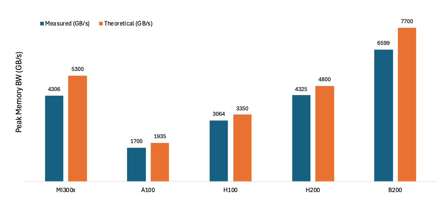
Paper's Figure 3, verbatim (caption: "Theoretical vs Measured Peak Memory BW").
MI300X achieves 4306 GB/s measured (81% of 5.3 TB/s theoretical), which is 1.41× H100's 3064 GB/s and essentially tied with H200's 4325 GB/s. This is MI300X's strongest relative dimension. NVIDIA achieves slightly higher utilization (86–91%) but MI300X's higher theoretical ceiling keeps its measured bandwidth competitive. The B200 note is interesting: it showed 10% improvement when re-benchmarked one month later, highlighting that all results are snapshots of rapidly moving software stacks.
| GPU | Measured BW | Theoretical BW | Utilization |
|---|---|---|---|
| MI300X | 4306 GB/s | 5300 GB/s | 81% |
| A100 | 1700 GB/s | 1935 GB/s | 88% |
| H100 | 3064 GB/s | 3350 GB/s | 91% |
| H200 | 4325 GB/s | 4800 GB/s | 90% |
| B200 | 6599 GB/s | 7700 GB/s | 86% |
Communication (8-GPU All-Reduce) #
| # GPUs | RCCL Measured (MI300X) | MI300X Theoretical | NCCL Measured (H100) | H100 Theoretical |
|---|---|---|---|---|
| 2 | 48 GB/s | 64 GB/s | 366 GB/s | 450 GB/s |
| 4 | 135 GB/s | 192 GB/s | 369 GB/s | 450 GB/s |
| 8 | 320 GB/s | 448 GB/s | 370 GB/s | 450 GB/s |
NCCL achieves ~85% utilization with uniform bandwidth at all GPU counts (NVSwitch). RCCL achieves ~70% with aggregate bandwidth scaling linearly (mesh). H100's NVSwitch advantage is most dramatic at 2 GPUs (366 vs 48 GB/s — 7.6×) and narrows at 8 GPUs (370 vs 320 GB/s — 1.16×) as the mesh topology accumulates more links.
End-to-end LLM inference (Llama 3.1 70B) #
| Regime | FP8 (MI300X / H100) | FP16 (MI300X / H100) |
|---|---|---|
| Prefill-dominated (short output) | ~50% | ~56% |
| Decode-dominated (output=2048) | ~66% | ~80% |
The prefill/decode split maps cleanly to §2/§3 findings: prefill is compute-bound where MI300X's 45% utilization deficit dominates; decode is memory-bound where MI300X's 4.3 TB/s BW advantage narrows the gap. FP16 outperforms FP8 in relative terms because FP16's doubled memory footprint pushes working sets into MI300X's higher-bandwidth array-size region (>64 MiB where MI300X saturates at ~4.3 TB/s vs lower BW for the small footprints typical of FP8).
§6 论证链 #
| Step | Claim | Evidence | Depends on |
|---|---|---|---|
| 1 | MI300X has 1.5× H100 theoretical FP8 compute (2615 vs 1979 TFLOPS) | Table 1: $304 \times 4096 \times 2.1\text{GHz}$ | — |
| 2 | MI300X achieves only 45% of peak (vs NVIDIA 82–97%) | Fig. 1: bar chart; Fig. 2: scaling curves | Step 1 |
| 3 | Clock throttles from 2100 to 1083–1217 MHz under sustained GEMM | Table 2: concurrent rocm-smi measurement | Step 2 (root cause #1) |
| 4 | After clock adjustment, software efficiency is 80–85% | Table 2: measured TFLOPS / (measured clock × CUs × Ops/cycle) | Step 3 (root cause #2) |
| 5 | Frequency × software efficiency ≈ observed utilization: $0.58 \times 0.82 \approx 0.48$ | Algebraic product of Steps 3 + 4 | Steps 3, 4 |
| 6 | Memory BW is MI300X's competitive dimension: 81% of 5.3 TB/s ≈ H200 | Fig. 3: measured vs theoretical across 5 GPUs | Independent |
| 7 | Mesh interconnect achieves 70% BW utilization vs NVSwitch 85% | §4.2: RCCL 320/448 vs NCCL 370/450 GB/s | Independent |
| 8 | E2E LLM inference maps to hardware profiles: prefill→compute gap, decode→memory parity | §5.1–5.2: MI300X at 37–66% (FP8) and 56–80% (FP16) of H100 | Steps 2, 5, 6 |
| 9 | FP16 narrows the gap because larger footprint enters MI300X's high-BW region | §5.2: FP16 doubles working set; Fig. 4 shows MI300X BW rises at >64 MiB | Steps 6, 8 |
| 10 | Overall gap is primarily software + power management, not hardware design | §6: software maturity is binding constraint; hardware $\eta_{\text{sw}}$ is 80–85% | Steps 3, 4, 5 |
§7 实现 cross-reference #
[实现未公开] — the paper uses existing vendor-provided tools without releasing custom analysis code: