AMD CDNA 2 Architecture White Paper
AMD CDNA 2 Architecture White Paper #
AMD | 2021-11 | https://www.amd.com/content/dam/amd/en/documents/instinct-business-docs/white-papers/amd-cdna2-white-paper.pdf Category: hardware | Tags: gpu-architecture, matrix-core, hpc, mi250x, cdna2, mcm, exascale Read: 2026-04-16
Core Contribution #
AMD首个多芯片模块(MCM)封装GPU架构CDNA 2,通过双GCD封装和CPU-GPU缓存一致性驱动全球首台Exascale超算Frontier。
Summary #
CDNA 2是AMD在计算GPU领域的重大跨越,首次采用多芯片模块(MCM)封装将两个GCD(Graphics Compute Die)通过interposer bridge以400GB/s双向带宽互联在同一封装内。每个GCD包含110个CU,双GCD合计220CU,配合FP64 Matrix Core的引入,实现了47.9 TFLOPS FP64 Vector和95.7 TFLOPS FP64 Matrix的惊人HPC性能,较MI100的11.5 TFLOPS实现4.2x飞跃。
显存升级至128GB HBM2e(3.2TB/s),L2 Cache扩大至16MB(8MB/GCD)。外部8条Infinity Fabric链路提供800GB/s互联带宽。关键创新包括与EPYC处理器的硬件级CPU-GPU缓存一致性、向量单元Packed FP32支持(有效翻倍FP32向量吞吐)、以及L2 FP64原子操作增强。
CDNA 2驱动了Frontier——世界首台Exascale超算,由9,408个MI250X节点组成,峰值超过1.1 ExaFLOPS FP64。
Key Findings #
- MCM封装: 双GCD通过interposer bridge互联,400GB/s封装内带宽
- FP64 Matrix Core: MFMA首次支持FP64矩阵运算,95.7 TFLOPS FP64 Matrix
- 220 CU (110/GCD), 128GB HBM2e, 3.2TB/s
- CPU-GPU缓存一致性: 与EPYC实现硬件级cache coherency
- 800GB/s外部IF链路(8 links),驱动Frontier Exascale超算
Key Tables #
Table 1: MI250X vs MI100 Performance Comparison #
| Computation | MI250X (双GCD) | MI100 | Speedup |
|---|---|---|---|
| FP64 Vector | 47.9 TFLOPS | 11.5 TFLOPS | 4.16x |
| FP64 Matrix | 95.7 TFLOPS | N/A | 新能力 |
| FP32 Matrix | 95.7 TFLOPS | 46.1 TFLOPS | 2.08x |
| FP16 Matrix | 383 TFLOPS | 184.6 TFLOPS | 2.07x |
| BF16 Matrix | 383 TFLOPS | 92.3 TFLOPS | 4.15x |
| INT8 Matrix | 383 TOPS | N/A | 新能力 |
| 显存容量 | 128 GB | 32 GB | 4x |
| 显存带宽 | 3.2 TB/s | 1.23 TB/s | 2.6x |
Takeaway: FP64性能实现4x+飞跃(MCM双die + FP64 Matrix Core),BF16通过对等FP16实现4x提升,显存容量4x
Table 2: MI250X 单GCD vs 双GCD规格 #
| 参数 | 单GCD | 双GCD (MI250X) |
|---|---|---|
| CU | 110 | 220 |
| FP64 Vector | 24.0 TFLOPS | 47.9 TFLOPS |
| FP64 Matrix | 47.9 TFLOPS | 95.7 TFLOPS |
| FP16 Matrix | 191.5 TFLOPS | 383 TFLOPS |
| 显存 | 64 GB HBM2e | 128 GB HBM2e |
| 显存带宽 | 1.6 TB/s | 3.2 TB/s |
| L2 Cache | 8 MB | 16 MB |
Takeaway: 双GCD实现近乎线性的性能扩展,封装内400GB/s互联保障了扩展效率
Limitations #
- 无FP8支持
- 无结构化稀疏
- 仍为7nm工艺,落后于同期NVIDIA 4N (H100)
- 双GCD在操作系统层面呈现为2个逻辑GPU,编程模型有额外复杂性
- 无Transformer Engine等AI专用加速
Infrastructure Impact #
- Algorithm: FP64 Matrix加速使科学计算矩阵运算全面受益
- Kernel: Packed FP32需要编译器/调度器适配
- Framework: ROCm + HIP持续追赶CUDA生态
- System: MCM封装开创GPU多die路线,Frontier验证Exascale可行性
- LLM: 128GB显存为早期大模型部署提供基础
Deep Analysis (hardware) #
Figure 1: MI200 Single GCD Block Diagram #
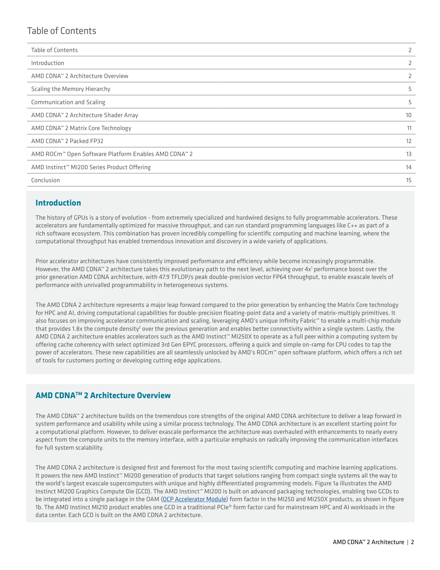
解读: AMD Instinct MI200单个Graphics Compute Die (GCD)的block diagram。每GCD包含4个Compute Engine(每Engine 28个CU, 共112 CU/GCD,产品启用110个)。中央是L2 Cache和Infinity Fabric互联。四周是Memory Controller和Memory PHY驱动HBM2e stacks。上方标注8条Infinity Fabric Links(7条GPU间互联 + 1条可配置为PCIe或IF)和2个VCN(Video Codec Next)编解码器。CU相比CDNA1增强了FP64 Matrix Core支持。
Figure 2: MI250X Dual-GCD MCM Package #
解读: MI250X多芯片模块(MCM)封装的完整block diagram。两个完整的GCD通过封装内Infinity Fabric以400GB/s双向带宽互联,形成统一的加速器。每GCD各有4个HBM2e stacks(64GB/GCD,总计128GB)。两GCD各有独立的8条Infinity Fabric链路用于外部连接。这是AMD首次在GPU中采用MCM封装——通过interposer bridge实现die间高速互联,在相同7nm工艺下将资源翻倍。OAM形态适配大规模HPC系统。
Figure 3: Flagship HPC Topology with MI250X #
解读: 旗舰HPC拓扑——MI250X + 优化版3rd Gen EPYC处理器的全系统连接方案(Frontier超算采用此设计)。4个MI250X(8 GCD)通过Infinity Fabric组成全互联拓扑。关键创新:(1)CPU-GPU之间通过coherent Infinity Fabric链路实现硬件级缓存一致性(非PCIe);(2)GPU拥有下行PCIe Root Complex,可直接连接NIC实现GPUDirect RDMA;(3)CPU和GPU作为对等计算资源,共享统一地址空间。这种拓扑驱动了ORNL Frontier成为全球首台Exascale超算。
Figure 4: CDNA2 Enhanced CU with FP64 Matrix Core #
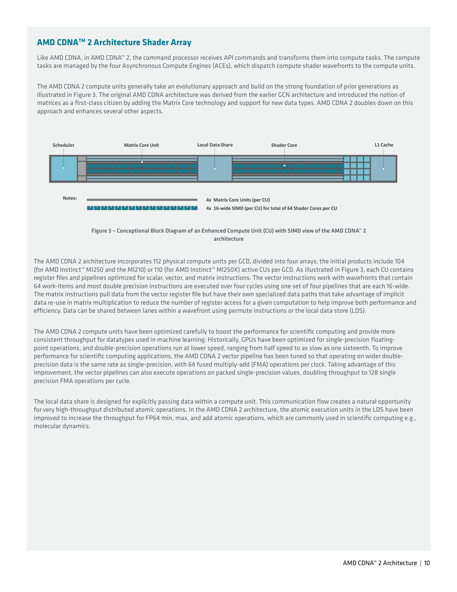
解读: CDNA 2架构CU内部结构图。相比CDNA 1的主要增强:(1)Matrix Core Engine新增FP64矩阵运算支持(MFMA FP64指令),使HPC应用也能利用矩阵加速达95.7 TFLOPS;(2)向量单元支持Packed FP32——在FP32宽度的数据通路中打包执行两个FP32操作,有效翻倍向量FP32吞吐;(3)L2原子操作增强——FP64 atomic add/min/max在L2 Cache执行,加速histogram等通信密集型算法。
1. Architecture Overview #
- 产品: AMD Instinct MI250X / CDNA 2
- 工艺: TSMC 7nm
- 封装: MCM — 2个GCD + interposer bridge
- 目标市场: Exascale HPC与AI训练
2. Generational Delta (vs CDNA 1 / MI100) #
新增: MCM双GCD封装, FP64 Matrix Core, Packed FP32, CPU-GPU缓存一致性, L2 FP64 atomic
移除: 无
增强: CU 220(vs 120), 显存128GB(vs 32GB), 带宽3.2TB/s(vs 1.23TB/s), IF链路800GB/s(vs 3x links)
3. Compute Unit Deep Dive #
- 每CU: 1个Matrix Core Engine (增加FP64 MFMA), 4个Vector单元(16-wide, 支持Packed FP32), Scalar单元
- VRF: 128KB/CU, SRF: 3.2KB/CU
- Wavefront: 64 work-items, \( C_{\text{wave}} = \frac{64}{16} = 4\ \text{cycles/wavefront} \)
- MFMA支持: FP64/FP32/FP16/BF16/INT8输入
- Stream Processors: \( N_{\text{SP}} = 220 \times 64 = 14{,}080 \)
Peak Performance Derivation (从第一性原理推导) #
\[ f_{\text{boost}} \approx 1.7\ \text{GHz} \]
\[ \text{FP16 Matrix} = 1024 \frac{\text{FLOPS}}{\text{clk} \cdot \text{CU}} \times 220\ \text{CU} \times 1.7\ \text{GHz} = 383\ \text{TFLOPS} \]
\[ \text{BF16 Matrix} = 1024 \frac{\text{FLOPS}}{\text{clk} \cdot \text{CU}} \times 220\ \text{CU} \times 1.7\ \text{GHz} = 383\ \text{TFLOPS} \quad (\text{same as FP16}) \]
\[ \text{FP64 Matrix} = 256 \frac{\text{FLOPS}}{\text{clk} \cdot \text{CU}} \times 220\ \text{CU} \times 1.7\ \text{GHz} = 95.7\ \text{TFLOPS} \]
\[ \text{FP32 Vector} = 128 \frac{\text{FLOPS}}{\text{clk} \cdot \text{CU}} \times 220\ \text{CU} \times 1.7\ \text{GHz} = 47.9\ \text{TFLOPS} \]
\[ \text{BW}_{\text{HBM}} = 1.6\ \text{GHz} \times 2 \times \frac{4096\ \text{bits/die} \times 2\ \text{dies}}{8} = 3.2\ \text{TB/s} \]
\[ \text{BW}_{\text{IF/link}} = 100\ \text{GB/s} \quad (300\ \text{GB/s} \div 3\ \text{in-package links}) \]
\[ \text{BW}_{\text{IF,ext}} = 8 \times 100\ \text{GB/s} = 800\ \text{GB/s} \]
4. Peak Performance #
| Data Type | Peak (单GCD) | Peak (双GCD MI250X) |
|---|---|---|
| FP64 Vector | 24.0 TFLOPS | 47.9 TFLOPS |
| FP64 Matrix | 47.9 TFLOPS | 95.7 TFLOPS |
| FP32 Matrix | 47.9 TFLOPS | 95.7 TFLOPS |
| FP16 Matrix | 191.5 TFLOPS | 383 TFLOPS |
| BF16 Matrix | 191.5 TFLOPS | 383 TFLOPS |
| INT8 Matrix | 191.5 TOPS | 383 TOPS |
5. Memory Subsystem #
- HBM2e: 128GB (64GB/GCD), 3.2TB/s (1.6TB/s/GCD)
- L2: 16MB (8MB/GCD), 32 slices/GCD
- Register: 128KB VRF/CU, 3.2KB SRF/CU
6. Interconnect #
- 封装内IF: 400GB/s双向 (interposer bridge)
- 外部IF链路: 800GB/s (8 links)
- PCIe Gen4: x16
- CPU-GPU缓存一致性: 与EPYC处理器硬件级coherent
7. Software & ISA #
- ROCm (持续迭代)
- MFMA指令族扩展: 新增FP64矩阵指令
- Packed FP32: 向量单元在FP32操作中可打包执行
- HIP + LLVM编译器