AMD CDNA 4 Architecture White Paper
AMD CDNA 4 Architecture White Paper #
AMD | 2025-06 | https://www.amd.com/content/dam/amd/en/documents/instinct-business-docs/white-papers/amd-cdna4-white-paper.pdf Category: hardware | Tags: gpu-architecture, matrix-core, chiplet, mi350x, mi355x, cdna4, mxfp, microscaling Read: 2026-04-16
Core Contribution #
AMD CDNA 4架构全面押注AI精度下探,引入MXFP Microscaling格式(MXFP8/6/4),矩阵资源翻倍,LDS扩容至160KB,在FP8达5 PFLOPS、MXFP4达10 PFLOPS,同时大胆移除TF32硬件并削减FP64 Matrix性能。
Summary #
CDNA 4是AMD对AI优先策略最明确的表态。架构从CDNA 3的8 XCD(5nm)+4 IOD(6nm)演进为8 XCD(3nm N3P)+2 IOD(6nm N6)——XCD升级至3nm获得更高密度和能效,IOD从4个精简为2个以降低功耗和延迟。256个CU(32/XCD)虽少于MI300X的304个,但per-CU矩阵吞吐翻倍(16-bit及以下数据类型),总AI性能实现大幅跃升。
核心创新是MXFP Microscaling格式支持——业界首批实现OCP MX标准的GPU,32个元素共享一个8-bit指数,提供MXFP8(E5M2/E4M3)、MXFP6(E3M2/E2M3)、MXFP4(E2M1)三个精度层级。MXFP6是AMD独有的中间精度,提供FP8和FP4之间的精度-性能折中。MI355X在FP8达5.0 PFLOPS,MXFP4/MXFP6达10 PFLOPS,较MI325X提升约3.85x(FP8基准)。
LDS从64KB扩容至160KB(2.5x),读带宽从128B/cycle翻倍至256B/cycle,大幅提升数据供给能力。Transcendental单元也2x以匹配矩阵吞吐增长。显存升级至288GB HBM3E(8.0TB/s)。
大胆取舍: TF32硬件移除(转为BF16软件模拟),FP64 Matrix性能减半(78.6 TFLOPS vs CDNA3的163.4 TFLOPS),腾出面积给MX格式和矩阵资源翻倍。这标志着AMD从HPC/AI双重定位明确转向AI优先。
Key Findings #
- 8 XCD(3nm N3P) + 2 IOD(6nm N6),IOD从4个缩减为2个
- 256 CU, FP8: 5.0 PFLOPS, MXFP4/MXFP6: 10 PFLOPS
- MXFP Microscaling: OCP MX标准, MXFP8/6/4三档精度
- LDS 160KB/CU (2.5x), 读带宽256B/cycle (2x)
- 288GB HBM3E, 8.0TB/s
- TF32硬件移除, FP64 Matrix减半 — AI优先的明确信号
- Matrix Core 16-bit及以下吞吐翻倍
Key Tables #
Table 1: MI355X / MI350X 完整性能规格 #
| Computation | MI350X (AC) | MI355X (DLC) | Sparsity (2:4) |
|---|---|---|---|
| Vector FP64 | 78.6 TFLOPS | 78.6 TFLOPS | - |
| Vector FP32 | 157.3 TFLOPS | 157.3 TFLOPS | - |
| Matrix FP64 | 78.6 TFLOPS | 78.6 TFLOPS | - |
| Matrix FP32 | 157.3 TFLOPS | 157.3 TFLOPS | - |
| Matrix FP16 | 2.5 PFLOPS | 2.5 PFLOPS | 5.0 PFLOPS |
| Matrix BF16 | 2.5 PFLOPS | 2.5 PFLOPS | 5.0 PFLOPS |
| Matrix FP8 | 5.0 PFLOPS | 5.0 PFLOPS | 10 PFLOPS |
| Matrix INT8 | 5.0 POPS | 5.0 POPS | 10 POPS |
| Matrix MXFP8 | 5.0 PFLOPS | 5.0 PFLOPS | 10 PFLOPS |
| Matrix MXFP6 | 10 PFLOPS | 10 PFLOPS | - |
| Matrix MXFP4 | 10 PFLOPS | 10 PFLOPS | - |
| 显存 | 288 GB HBM3E | 288 GB HBM3E | - |
| 显存带宽 | 8.0 TB/s | 8.0 TB/s | - |
| TDP | 1000W | 1400W | - |
| 冷却 | 风冷 | 液冷 | - |
Takeaway: MI350X与MI355X计算性能完全一致,差异仅在散热(风冷vs液冷)和TDP(1000W vs 1400W)
Table 2: MI355X vs MI325X 代际对比 #
| 指标 | MI355X (CDNA4) | MI325X (CDNA3) | 提升 |
|---|---|---|---|
| 工艺 | 3nm+6nm | 5nm+6nm | XCD升级 |
| CU | 256 | 304 | 0.84x (减少) |
| FP64 Matrix | 78.6 TF | 163.4 TF | 0.48x (减半!) |
| FP32 Matrix | 157.3 TF | 163.4 TF | 0.96x (持平) |
| FP16 Matrix | 2,516 TF | 1,307 TF | 1.92x |
| FP8 Matrix | 5,033 TF | 2,615 TF | 1.93x |
| MXFP4 | 10,066 TF | N/A | 新能力 |
| 显存 | 288 GB | 256 GB | 1.13x |
| 带宽 | 8.0 TB/s | 6.0 TB/s | 1.33x |
| LDS/CU | 160 KB | 64 KB | 2.5x |
Takeaway: CU减少但per-CU矩阵吞吐翻倍(16-bit以下),FP64 Matrix被主动牺牲,MXFP4为全新能力
Table 3: MI355X vs B200 竞争对比 #
| 指标 | MI355X | B200 (est.) | 对比 |
|---|---|---|---|
| FP64 Matrix | 78.6 TF | ~90 TF | NVIDIA |
| FP16 TC | 2,516 TF (5,033 sparse) | ~2,500 TF (~5,000 sparse) | 接近 |
| FP8 TC | 5,033 TF (10,066 sparse) | ~5,000 TF (~10,000 sparse) | 接近 |
| MXFP6 | 10,066 TF | N/A | AMD独有 |
| MXFP4/FP4 | 10,066 TF | ~10,000 TF | 接近 |
| 显存 | 288 GB | 192 GB | AMD +50% |
| 带宽 | 8.0 TB/s | 8.0 TB/s | 平局 |
| 互联 | 1,075 GB/s IF | 1,800 GB/s NVLink5 | NVIDIA +67% |
| NVLink域 | 8 GPU | 72 GPU (NVL72) | NVIDIA 9x |
| TDP | 1,400W | 1,000W | NVIDIA更优 |
Takeaway: FP8/FP16峰值基本持平(~5 PFLOPS),AMD保持显存优势(+50%),NVIDIA在互联(+67%)和规模化(NVL72)上领先
Limitations #
- TF32硬件移除,转为BF16软件模拟,兼容性和性能可能受影响
- FP64 Matrix性能减半(78.6 vs 163.4 TFLOPS),HPC用户受损
- CU数量减少(256 vs 304),依赖per-CU吞吐翻倍弥补
- TDP 1400W(DLC)功耗极高
- 互联带宽(1,075GB/s)落后NVLink5(1,800GB/s) 67%
- 缺乏NVL72等价的机架级GPU直联方案,大规模训练扩展性受限
Infrastructure Impact #
- Algorithm: MXFP6提供FP8/FP4之间的精度-性能新折中,需要量化算法适配
- Kernel: LDS 160KB + 256B/cycle允许更大tile size和更高数据复用
- Framework: MX格式需要PyTorch/JAX框架层面的量化支持
- LLM: 288GB显存 + 10 PFLOPS MXFP4,单卡可推理更大模型,更低精度
- System: IOD缩减为2个简化了系统设计,但互联带宽差距需要网络层弥补
Deep Analysis (hardware) #
Analyst perspective: senior hardware architect with tape-out experience. All FLOPS numbers derived from first principles and cross-checked against official specs.
1. Architecture Overview & Naming #
| Parameter | Value |
|---|---|
| Product Family | AMD Instinct MI350 Series |
| SKUs | MI350X (air-cooled, 1000W) / MI355X (liquid-cooled, 1400W) |
| Architecture | AMD CDNA 4 |
| ISA Code | gfx950 |
| Process — XCD | TSMC N3P (3nm, cutting-edge logic density) |
| Process — IOD | TSMC N6 (6nm, cost-effective for SRAM/IO) |
| Transistor Count | 185 billion (across all 10 chiplets) |
| Packaging | 3D chiplet — 8 XCD stacked vertically on 2 IOD via advanced packaging |
| Chiplet Composition | 8 XCD (compute) + 2 IOD (memory/cache/IO) + 8 HBM3E stacks |
| Target Market | Datacenter AI training & inference (AI-first, HPC secondary) |
Figure 1: Advanced 3D Package Construction #
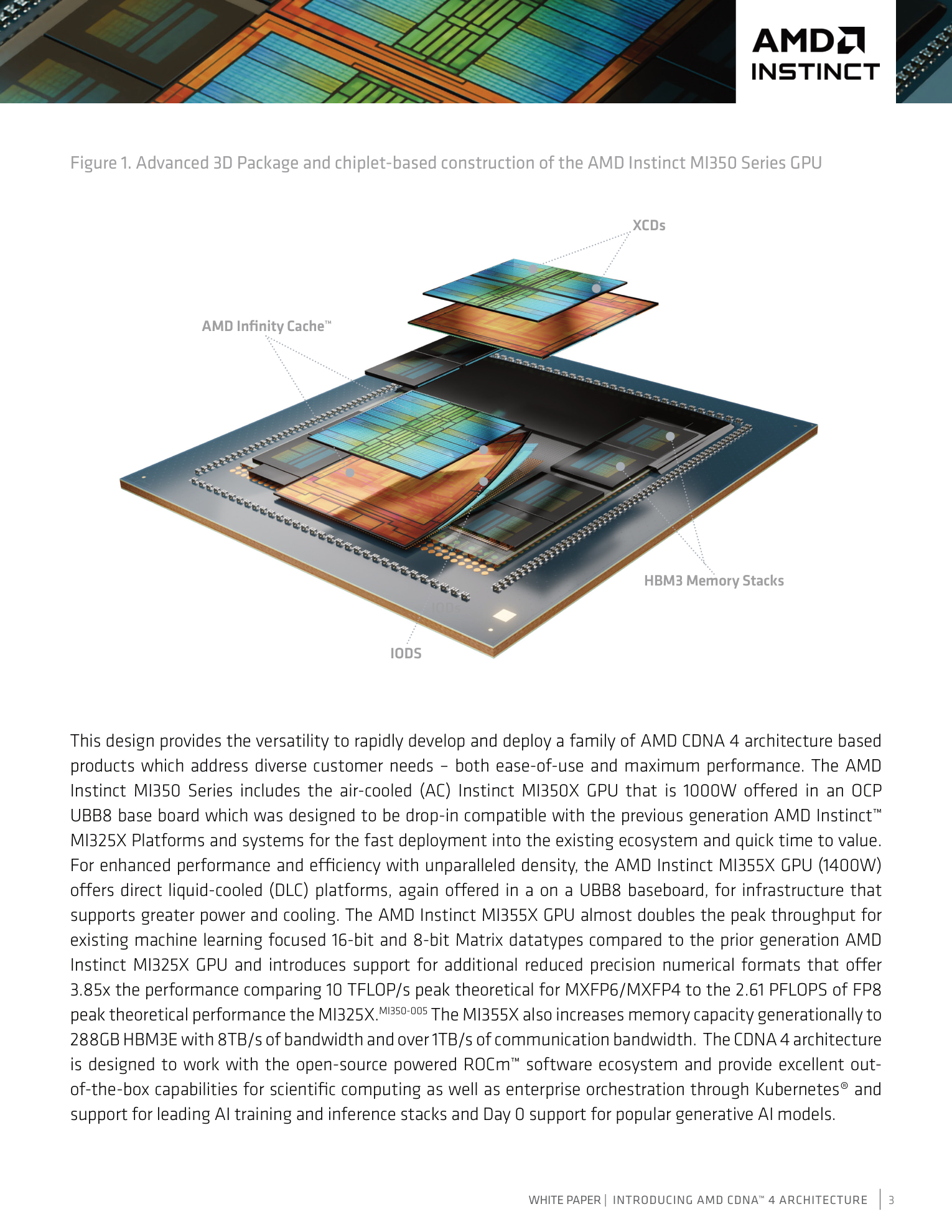
解读: 这张图展示了MI350 Series GPU的3D封装结构。8个XCD compute chiplet (绿色) 垂直堆叠在2个IOD (蓝色) 上方,四周环绕8个HBM3E内存堆栈。IOD之间通过Infinity Fabric直连。IOD内部包含Infinity Cache (256MB total)、内存控制器、以及对外的Infinity Fabric链路和PCIe Gen5接口。这种异构3D封装是CDNA 4的核心物理架构——XCD使用最先进的N3P工艺获取逻辑密度和能效,IOD使用成熟的N6工艺降低成本(SRAM和IO不从先进工艺获益)。相比CDNA 3的4个IOD方案,2个IOD简化了片上Infinity Fabric网络拓扑,降低了跨IOD通信延迟约14%并节省功耗。
设计哲学: CDNA 4证明了chiplet异构集成的第二代优势——在同一封装内独立优化计算die和IO die的工艺节点、面积、功能分配。XCD从N5→N3P获得密度和频率提升,IOD保持N6但从4个合并为2个,减少了die-to-die通信跳数,这是一个精巧的"减法"优化。
2. Generational Delta (vs CDNA 3 — MI300X/MI325X) #
2a. 新增单元 (Added) #
| New Feature | Description | Why it matters for AI |
|---|---|---|
| MXFP8 Matrix (E5M2/E4M3 + shared exp) | OCP MX microscaling — 32 elements share 1 eight-bit exponent | Per-block scaling >> per-tensor scaling; enables FP8-class GEMM on tensors that previously required FP16 due to outlier range |
| MXFP6 Matrix (E3M2/E2M3 + shared exp) | 6-bit microscaled format — AMD-unique mid-precision | Sweet spot: same 10 PF throughput as MXFP4 but 50% more mantissa bits; better accuracy than FP4 at no perf cost |
| MXFP4 Matrix (E2M1 + shared exp) | 4-bit microscaled format | Maximum throughput (10 PF); enables aggressive weight quantization for inference |
| 2× Matrix Core resources (≤16-bit) | Doubled MFMA execution width for FP16/BF16/FP8/INT8 | Per-CU AI throughput doubles, compensating for reduced CU count |
| 2× Transcendental rate | Doubled SFU throughput for exp/log/recip | Directly benefits softmax in attention; prevents transcendental from becoming bottleneck as matrix rate doubles |
| LDS direct load from L1 | Data can flow L1 → LDS without transiting VGPRs | Reduces VGPR pressure and latency for matrix multiply data staging |
| Data conversion instructions | New ISA instructions for MX format encode/decode | Enables efficient on-the-fly conversion between FP16/BF16 and MXFP6/4 in kernels |
2b. 删除/移除 (Removed) #
| Removed Feature | Reason | Impact |
|---|---|---|
| TF32 hardware | Area reclaimed for MX format circuits; TF32 usage declining in ecosystem | Supported via BF16 software emulation — same model accuracy, \(\sim 2\times\) slower than native TF32 would be. Acceptable trade because BF16 Matrix at 2.5 PF exceeds CDNA3's TF32 at 490 TFLOPS |
| 2 IODs (4→2) | Simplify fabric, reduce power, lower latency | Fewer die-to-die hops; NUMA modes change (NPS4→NPS2 max); per-IOD HBM stacks remain 4 |
| FP64 Matrix halved (\(256 \to 128\ \text{FLOPS/clk/CU}\)) | Area rebalanced from FP64 MFMA toward sub-8-bit MAC | FP64 Matrix drops from 163.4 TF to 78.6 TF — a deliberate signal that CDNA 4 is AI-first, not HPC-first |
2c. 增强/升级 (Enhanced) #
| Enhanced Unit | CDNA 3 | CDNA 4 | Improvement | How measured |
|---|---|---|---|---|
| XCD process | TSMC N5 | TSMC N3P | ~1 node jump | Higher logic density, better freq/W |
| LDS capacity | 64 KB/CU | 160 KB/CU | 2.5× | Banks increased |
| LDS read bandwidth | 128 B/clk | 256 B/clk | 2× | Measured per CU |
| HBM capacity | 192/256 GB | 288 GB | 1.13–1.5× | \(36\ \text{GB/stack} \times 8\ \text{stacks}\) |
| HBM bandwidth | 5.3/6.0 TB/s | 8.0 TB/s | 1.33–1.51× | 8 Gbps per pin (vs 6.0 Gbps) |
| Infinity Fabric link speed | 32 Gbps | 38.4 Gbps | +20% | Per-lane signaling rate |
| P2P aggregate BW | 896 GB/s | 1,075.2 GB/s | +20% | \(7 \times 76.8\ \text{GB/s} \times 2\) |
| IOD bisection BW | ~4.8 TB/s (est.) | 5.5 TB/s | +14% | Inter-IOD direct link |
| L2 coherency | Standard writeback | +non-coherent DRAM caching, dirty writeback w/ retained copy | Incremental | Reduces unnecessary evictions |
| Instruction cache | 64 KB/2 CUs, 8-way | Same | Unchanged | — |
2d. 架构级变更 (Architectural Changes) #
- CU count reduced: \(304 \to 256\) (\(38 \to 32\)/XCD). Each XCD fabricates 36 CUs in 4 arrays of 9; 4 disabled for yield. The per-CU throughput doubling (≤16-bit) more than compensates at the chip level for AI workloads.
- IOD repartitioning: 4 IODs → 2 larger IODs. Each IOD now contains 4 HBM controllers, 128 MB Infinity Cache, and 4 IF links. The direct connection between the two IODs is simpler and ~14% faster than the 4-IOD mesh in CDNA 3.
- NUMA topology simplified: NPS4 (4 NUMA zones) no longer available; max is NPS2 (2 zones, 1 per IOD) or NPS1 (flat). DPX+NPS2 is the recommended efficient operating mode.
- Matrix Core internal pipeline: Execution resources doubled for ≤16-bit types. The MFMA instruction set is extended with new opcodes for MXFP8/MXFP6/MXFP4 operands. FP64 MFMA execution width halved.
- L2 cache: Unchanged 4MB/XCD (32MB total), but gains coherency optimizations — can now cache non-coherent DRAM data and writeback dirty lines while retaining a clean copy.
3. Compute Unit Deep Dive #
3a. Compute Unit Structure #
Full GPU totals: \(256\) CUs (\(32/\text{XCD} \times 8\ \text{XCDs}\)), \(16{,}384\) Stream Processors (\(64/\text{CU}\)), \(1{,}024\) Matrix Cores (\(4/\text{CU} \times 256\ \text{CUs}\))
┌──────────────────────────────────────────────────────────┐
│                    CDNA 4 Compute Unit                    │
│                                                          │
│  ┌──────────────┐  ┌───────────────────────────────────┐ │
│  │ Scalar Unit  │  │ Vector Unit (VALU)                │ │
│  │  SALU pipe   │  │  4× 16-wide SIMD = 64 SPs        │ │
│  │  SGPRs       │  │  FP64/FP32/FP16/INT32 ops        │ │
│  └──────────────┘  │  VGPRs: 512 × 32-bit registers   │ │
│                     └───────────────────────────────────┘ │
│  ┌───────────────────────────────────────────────────────┐│
│  │ Matrix Core Engine (4 Matrix Cores)                   ││
│  │  2× execution resources for ≤16-bit (vs CDNA3)       ││
│  │  MFMA instructions: FP64/FP32/FP16/BF16/FP8/INT8    ││
│  │                     MXFP8/MXFP6/MXFP4 (NEW)         ││
│  │  Accumulator: FP32 (for all ≤16-bit types)           ││
│  │  AGPRs (Accumulator GPRs): 512 × 32-bit              ││
│  └───────────────────────────────────────────────────────┘│
│  ┌──────────────┐  ┌──────────────────────────────────┐  │
│  │ Transcendental│  │ Load/Store Unit                  │  │
│  │ SFU: 2× rate │  │ Memory pipeline                  │  │
│  │ exp,log,rcp  │  │ 128B cache line granularity      │  │
│  └──────────────┘  └──────────────────────────────────┘  │
│  ┌──────────────┐  ┌──────────────────────────────────┐  │
│  │ L1 Data Cache│  │ Local Data Share (LDS)            │  │
│  │  32 KB       │  │  160 KB  (was 64 KB)             │  │
│  │  128B lines  │  │  256 B/clk read BW (was 128)     │  │
│  │  64-way SA   │  │  Direct load from L1 (NEW)       │  │
│  └──────────────┘  └──────────────────────────────────┘  │
│  Instruction Cache: 64 KB shared between 2 adjacent CUs  │
│  Wavefront: 64 work-items                                │
└──────────────────────────────────────────────────────────┘
Figure 2: XCD Block Diagram #
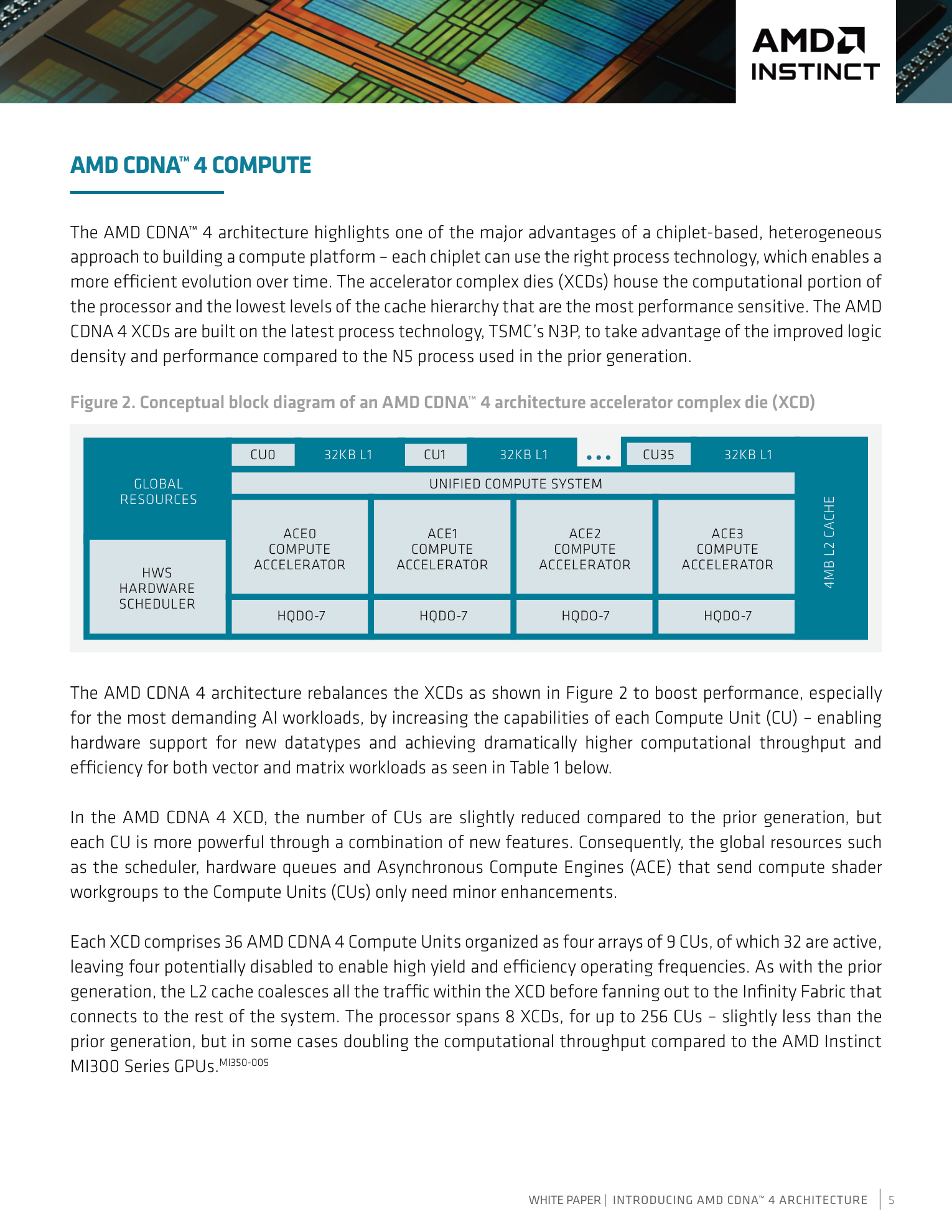
解读: 这张图展示了单个CDNA 4 XCD (Accelerator Complex Die) 的概念框图。每个XCD包含32个活跃CU(从36个中禁用4个保良率),被组织为4个CU阵列。全局资源包括硬件调度器(HWS)、4个异步计算引擎(ACE0-ACE3),每个ACE管理最多8个硬件队列(HQDO-7)。所有CU共享4MB L2 Cache,L2是XCD与Infinity Fabric网络的网关。32 KB L1 Data Cache标注在每个CU旁边。这个层级结构说明了工作分发路径: HWS → ACE → CU workgroup dispatch,以及数据路径: CU L1 → XCD L2 → Infinity Fabric → IOD。
3b. Matrix Core Specifications (per CU) #
From whitepaper Table 1, FLOPS/clock/CU data:
| Data Type | Input → Output | FLOPS/clk/CU (CDNA3) | FLOPS/clk/CU (CDNA4) | Change |
|---|---|---|---|---|
| FP64 Matrix | FP64 → FP64 | 256 | 128 | 0.5× (halved) |
| FP32 Matrix | FP32 → FP32 | 256 | 256 | 1× |
| FP16 Matrix | FP16 → FP32 | 2,048 | 4,096 | 2× |
| BF16 Matrix | BF16 → FP32 | 2,048 | 4,096 | 2× |
| FP8 Matrix (OCP) | E4M3/E5M2 → FP32 | 4,096 | 8,192 | 2× |
| INT8 Matrix | INT8 → INT32 | 4,096 | 8,192 | 2× |
| MXFP8 Matrix | MXFP8 → FP32 | N/A | 8,192 | New |
| MXFP6 Matrix | MXFP6 → FP32 | N/A | 16,384 | New |
| MXFP4 Matrix | MXFP4 → FP32 | N/A | 16,384 | New |
Vector units (unchanged per CU):
| Data Type | FLOPS/clk/CU (CDNA3) | FLOPS/clk/CU (CDNA4) |
|---|---|---|
| FP64 Vector | 128 | 128 |
| FP32 Vector | 256 | 256 |
| FP16 Vector | 256 | 256 |
Key observation on MXFP6 = MXFP4 throughput: Both achieve 16,384 FLOPS/clk/CU — identical throughput despite MXFP6 having 50% more bits per element (6 vs 4). This strongly suggests the sub-byte Matrix Core datapath operates at a fixed 4-bit element granularity internally. MXFP6 elements likely occupy the same MAC array slots as MXFP4 elements (padded or decomposed). This makes MXFP6 the strict sweet spot: same throughput as MXFP4 with materially better numerical precision (E3M2 has \(3\times\) the mantissa resolution of E2M1).
Sparsity (2:4 structured): Doubles effective throughput for FP16/BF16/FP8/INT8/MXFP8. The hardware skips zero-valued elements in a 2:4 pattern within each group of 4 elements. Note that MXFP6 and MXFP4 sparsity is NOT listed in the whitepaper, suggesting these formats do not support sparsity acceleration.
4. Peak Performance Derivation — From First Principles #
4a. Derivation Formula #
\[ \text{Peak TFLOPS} = N_{\text{CU}} \times \frac{\text{FLOPS}}{\text{clk} \cdot \text{CU}} \times f_{\text{clk}} \]
where:
- \( N_{\text{CU}} = 256 \) (\( 32\ \text{per XCD} \times 8\ \text{XCDs} \))
- \( \frac{\text{FLOPS}}{\text{clk} \cdot \text{CU}} \) from Table 1 (includes Matrix Core contributions)
- \( f_{\text{clk}} = 2.4\ \text{GHz} \) (MI355X) or \( 2.2\ \text{GHz} \) (MI350X)
4b. MI355X Derivation (2.4 GHz boost clock) #
| Data Type | FLOPS/clk/CU | × CUs | × GHz | = TFLOPS | Official | Match? |
|---|---|---|---|---|---|---|
| Vector FP64 | 128 | 256 | 2.4 | 78.6 TF | 78.6 TF | ✓ |
| Vector FP32 | 256 | 256 | 2.4 | 157.3 TF | 157.3 TF | ✓ |
| Vector FP16 | 256 | 256 | 2.4 | 157.3 TF | 157.3 TF | ✓ |
| Matrix FP64 | 128 | 256 | 2.4 | 78.6 TF | 78.6 TF | ✓ |
| Matrix FP32 | 256 | 256 | 2.4 | 157.3 TF | 157.3 TF | ✓ |
| Matrix FP16 | 4,096 | 256 | 2.4 | 2,516 TF ≈ 2.5 PF | 2.5 PF | ✓ |
| Matrix BF16 | 4,096 | 256 | 2.4 | 2,516 TF ≈ 2.5 PF | 2.5 PF | ✓ |
| Matrix FP8 | 8,192 | 256 | 2.4 | 5,033 TF ≈ 5.0 PF | 5.0 PF | ✓ |
| Matrix INT8 | 8,192 | 256 | 2.4 | 5,033 TOPs ≈ 5.0 PO | 5.0 POPs | ✓ |
| Matrix MXFP8 | 8,192 | 256 | 2.4 | 5,033 TF ≈ 5.0 PF | 5.0 PF | ✓ |
| Matrix MXFP6 | 16,384 | 256 | 2.4 | 10,066 TF ≈ 10 PF | 10 PF | ✓ |
| Matrix MXFP4 | 16,384 | 256 | 2.4 | 10,066 TF ≈ 10 PF | 10 PF | ✓ |
Whitepaper typo note: Table 1 lists MXFP6/MXFP4 as "16834" FLOPS/clk/CU. This is a typographical error; the correct value is 16,384 (\(= 2^{14}\)). Proof: \(16{,}384 \times 256 \times 2.4 = 10{,}066\ \text{TFLOPS} \approx 10\ \text{PF}\) (matches official spec). The erroneous "16,834" would yield \(10{,}342\ \text{TFLOPS}\) which does not match.
4c. MI350X Derivation (2.2 GHz boost clock) #
| Data Type | FLOPS/clk/CU | × CUs | × GHz | = TFLOPS | Official | Match? |
|---|---|---|---|---|---|---|
| Vector FP64 | 128 | 256 | 2.2 | 72.1 TF | 72.1 TF | ✓ |
| Vector FP32 | 256 | 256 | 2.2 | 144.2 TF | 144.2 TF | ✓ |
| Matrix FP64 | 128 | 256 | 2.2 | 72.1 TF | 72.1 TF | ✓ |
| Matrix FP16 | 4,096 | 256 | 2.2 | 2,307 TF ≈ 2.3 PF | 2.3 PF | ✓ |
| Matrix FP8 | 8,192 | 256 | 2.2 | 4,614 TF ≈ 4.6 PF | 4.6 PF | ✓ |
| Matrix MXFP4 | 16,384 | 256 | 2.2 | 9,227 TF ≈ 9.2 PF | 9.2 PF | ✓ |
MI350X vs MI355X: the only difference is clock speed (\(2.2\ \text{vs}\ 2.4\ \text{GHz} = 0.917\times\) ratio). All per-CU resources, CU count, memory, and IO are identical.
4d. Sparsity Multiplier #
2:4 structured sparsity doubles effective throughput for FP16/BF16/FP8/INT8/MXFP8:
| Precision | Dense Peak (MI355X) | With 2:4 Sparsity |
|---|---|---|
| FP16 Matrix | 2.5 PF | 5.0 PF |
| BF16 Matrix | 2.5 PF | 5.0 PF |
| FP8 Matrix | 5.0 PF | 10 PF |
| INT8 Matrix | 5.0 POPs | 10 POPs |
MXFP6 and MXFP4 do not list sparsity support in the whitepaper — these formats already achieve 10 PF dense, equaling FP8 with sparsity. The sub-byte element packing likely makes 2:4 sparsity metadata impractical.
4e. Generational Comparison (MI355X vs MI300X) #
| Metric | MI300X (CDNA3) | MI355X (CDNA4) | Ratio | Source of Change |
|---|---|---|---|---|
| CU count | 304 | 256 | 0.84× | 38→32 CU/XCD |
| Boost clock | 2.1 GHz | 2.4 GHz | 1.14× | N5→N3P process |
| FP64 Matrix | 163.4 TF | 78.6 TF | 0.48× | FLOPS/clk halved + fewer CUs |
| FP32 Matrix | 163.4 TF | 157.3 TF | 0.96× | Same FLOPS/clk, fewer CUs, higher freq |
| FP16 Matrix | 1,307 TF | 2,516 TF | 1.93× | \(2\times\) FLOPS/clk, partially offset by \(0.84\times\) CUs |
| FP8 Matrix | 2,615 TF | 5,033 TF | 1.93× | Same mechanism |
| MXFP4 | N/A | 10,066 TF | ∞ (new) | Entirely new capability |
Why 1.93× not 2×? The per-CU throughput doubles, but CU count drops from 304 to 256 (\(0.842\times\)) while clock rises from 2.1 to 2.4 GHz (\(1.143\times\)). Net: \(2.0 \times 0.842 \times 1.143 = \mathbf{1.924\times}\). This matches the whitepaper's "~1.9x" claim precisely.
5. Memory Subsystem #
5a. HBM Specifications #
| Parameter | Value |
|---|---|
| Memory Type | HBM3E (12-Hi stacks) |
| Memory Capacity | 288 GB (36 GB × 8 stacks) |
| Stacks | 8 (4 per IOD) |
| Bus Width per Stack | 1,024 bits |
| Data Rate | 8 Gbps per pin |
| Total Memory Bandwidth | 8.0 TB/s |
Bandwidth derivation:
\[
\begin{aligned}
\text{BW} &= \frac{W_{\text{bus}} \times R_{\text{data}} \times N_{\text{stacks}}}{8\ \text{bits/byte}} \\
&= \frac{1{,}024\ \text{bits} \times 8\ \text{Gbps} \times 8\ \text{stacks}}{8} \\
&= \frac{65{,}536\ \text{Gbps}}{8} = 8{,}192\ \text{GB/s} \approx 8.0\ \text{TB/s} \quad \checkmark
\end{aligned}
\]
vs CDNA 3 (MI325X): \(6.0 \to 8.0\ \text{TB/s} = \mathbf{+33\%}\) (from \(6 \to 8\ \text{Gbps}\) per pin).
Figure 5: Multi-Die Chiplet Memory and I/O System #
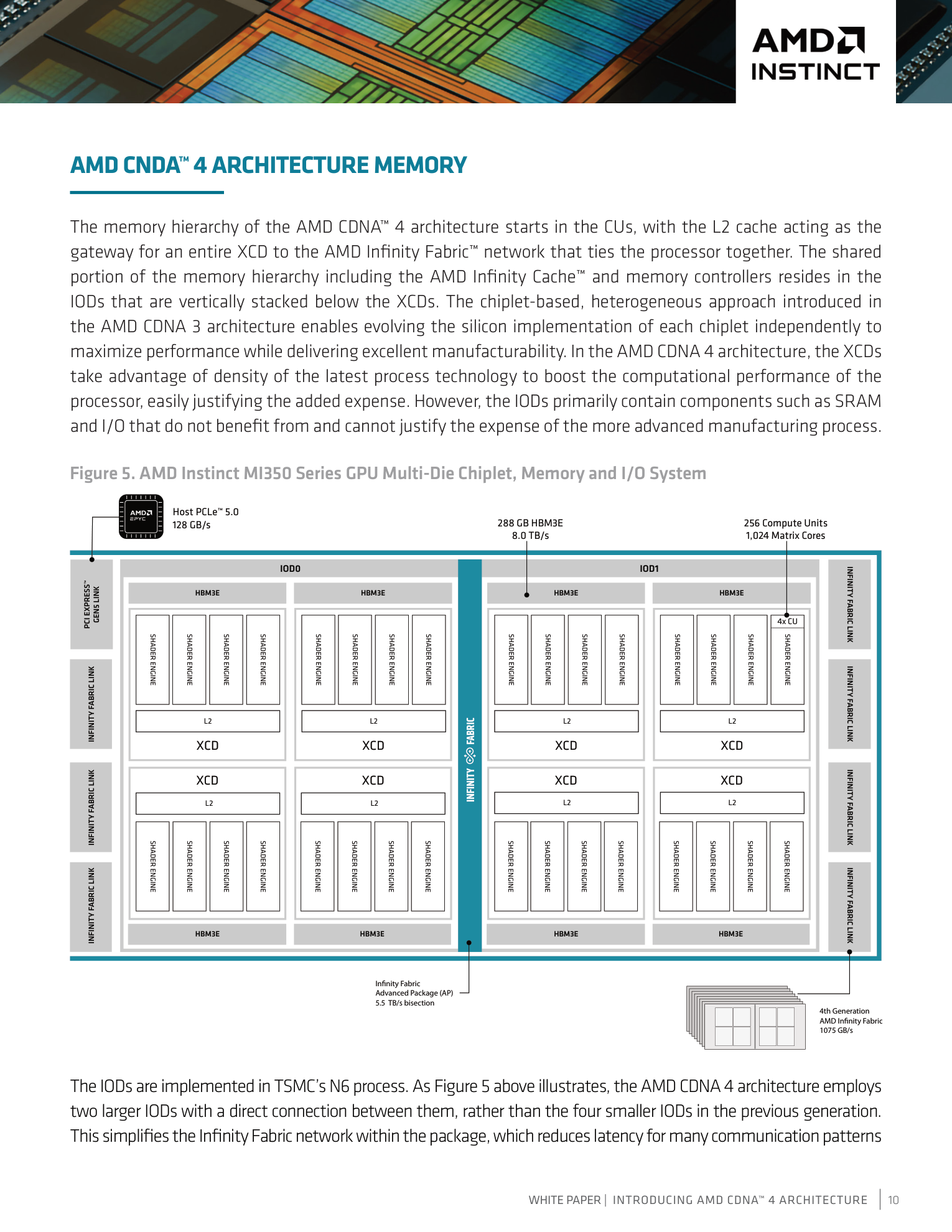
解读: 这是CDNA 4架构最关键的一张图,展示了完整的memory和IO子系统拓扑。关键信息:
- 2个IOD (上方IOD0,下方IOD1) 通过Infinity Fabric直连,bisection带宽5.5 TB/s
- 每个IOD连接4个HBM3E堆栈 (每侧2个),总计8个堆栈 = 288 GB
- 每个IOD包含128MB Infinity Cache (16-way set-associative memory-side cache)
- 8个XCD (4个在每个IOD上方) 通过3D堆叠垂直连接到IOD
- 对外接口: 7条Infinity Fabric链路 (每个IOD 3-4条) 用于GPU间通信,1条PCIe Gen5 x16连接host CPU
- 图中标注了关键带宽数字: 288 GB HBM3E @ 8.0 TB/s, 256 CU / 1,024 Matrix Cores, 5.5 TB/s bisection, 1,075 GB/s P2P, 128 GB/s PCIe
- 与CDNA 3的4-IOD设计对比: 2-IOD简化了Infinity Fabric网络拓扑,减少了XCD访问远端IOD的跳数。在CDNA 3中,CU到远端IOD可能需要经过中间IOD的两次Infinity Fabric跳转;在CDNA 4中最多1次跳转(通过IOD间直连)。
5b. Cache Hierarchy #
| Level | Capacity | Organization | Key Specs | Shared/Private |
|---|---|---|---|---|
| L1 Data Cache | 32 KB/CU | 64-way set-associative, 128B lines | Per-CU, within CU memory pipeline | Per CU (private) |
| LDS (Local Data Share) | 160 KB/CU | Banked, directly addressed | 256 B/clk read BW, L1→LDS direct load | Per CU (explicitly managed) |
| Instruction Cache | 64 KB/2 CUs | 8-way set-associative | Shared between 2 adjacent CUs | Shared (2 CUs) |
| L2 Cache | 4 MB/XCD (32 MB total) | 16-way SA, 16 channels | 128B read + 64B write per channel/cycle; writeback + write-allocate; can cache non-coherent DRAM | Per XCD (shared by 32 CUs) |
| Infinity Cache (LLC) | 256 MB total (128 MB/IOD) | 16-way SA, memory-side cache | 16 channels × 64B wide per HBM stack, 128 channels total | Shared (global) |
LDS deep dive: The LDS expansion from 64 KB to 160 KB is one of the most impactful changes for kernel performance. The CDNA 3 LDS had \(32\ \text{banks} \times 512\ \text{entries} \times 4\ \text{bytes} = 64\ \text{KB}\). CDNA 4 increases both bank count and depth to reach 160 KB, while doubling read bandwidth to 256 B/clk. The new L1→LDS direct load path eliminates the need to stage data through VGPRs, saving both register pressure and instruction count. For a typical GEMM tile: 160 KB LDS can hold a \(256 \times 128\) FP16 tile (64 KB) plus a \(128 \times 256\) FP16 tile (64 KB) with 32 KB headroom for metadata/pointers — vs CDNA 3 which could barely fit one such tile pair.
5c. Ops:Byte Ratio (Arithmetic Intensity Ridge Points) #
\[ \beta_{\text{Ops:Byte}} = \frac{\text{Peak TFLOPS}}{\text{Memory BW (TB/s)}} \]
| Precision | Peak TFLOPS | HBM BW (TB/s) | Ops:Byte | Implication |
|---|---|---|---|---|
| MXFP4 Matrix | 10,066 | 8.0 | 1,258 | Only massive GEMMs are compute-bound |
| MXFP6 Matrix | 10,066 | 8.0 | 1,258 | Same — MXFP6 has same throughput |
| FP8 Matrix | 5,033 | 8.0 | 629 | Large GEMM compute-bound; attention memory-bound |
| FP16 Matrix | 2,516 | 8.0 | 315 | Standard training precision ridge point |
| FP32 Vector | 157.3 | 8.0 | 19.7 | Almost everything compute-bound |
| FP64 Vector | 78.6 | 8.0 | 9.8 | HPC ops mostly compute-bound |
Practical meaning: At FP8 with \(\beta = 629\), a GEMM needs arithmetic intensity \(\geq 629\) to be compute-bound. For a square GEMM of size \(M = N = K\), arithmetic intensity \(\approx M/2\), so \(M \geq 1{,}258\) is needed. For MXFP4 (\(\beta = 1{,}258\)), \(M \geq 2{,}516\). This means:
- Prefill (large batch, large M): typically compute-bound ✓
- Decode (batch=1, M=1): always memory-bound — bandwidth is the bottleneck
- Attention: memory-bound for most sequence lengths (arithmetic intensity \(\sim \text{seq\_len}\), and \(\text{seq\_len} < 1{,}258\) for most practical cases)
- Elementwise ops (LayerNorm, activation): \(\sim 1\text{-}2\ \text{ops/byte}\) → always memory-bound
6. Interconnect & I/O #
6a. External Interconnect #
| Link Type | Count | Width | Speed | Per-Link BW (per dir) | Per-Link BW (bidir) |
|---|---|---|---|---|---|
| Infinity Fabric Link | 7 | 16-bit | 38.4 Gbps | 76.8 GB/s | 153.6 GB/s |
| PCIe Gen 5 | 1 | x16 | 32 GT/s | 64 GB/s | 128 GB/s |
Derivation:
\[
\begin{aligned}
R_{\text{per-link}} &= \frac{16\ \text{bits} \times 38.4\ \text{Gbps}}{8} = 76.8\ \text{GB/s} \\
R_{\text{bidir}} &= 76.8 \times 2 = 153.6\ \text{GB/s} \\
R_{\text{P2P}} &= 7 \times 153.6 = 1{,}075.2\ \text{GB/s} \quad \checkmark \\
R_{\text{total}} &= 1{,}075.2 + 128 = 1{,}203.2\ \text{GB/s} \quad \checkmark
\end{aligned}
\]
vs CDNA 3: \(8 \times 32\ \text{Gbps} \times 16\ \text{bits} / 8 \times 2 = 1{,}024\ \text{GB/s}\) total → but only 7 for P2P \(= 896\ \text{GB/s}\). CDNA 4 P2P BW \(= 1{,}075.2 / 896 = \mathbf{+20\%}\) improvement, entirely from the \(32 \to 38.4\ \text{Gbps}\) signaling rate increase.
6b. Scale-Up Topology #
Figure 7: 8-GPU Platform Topology #
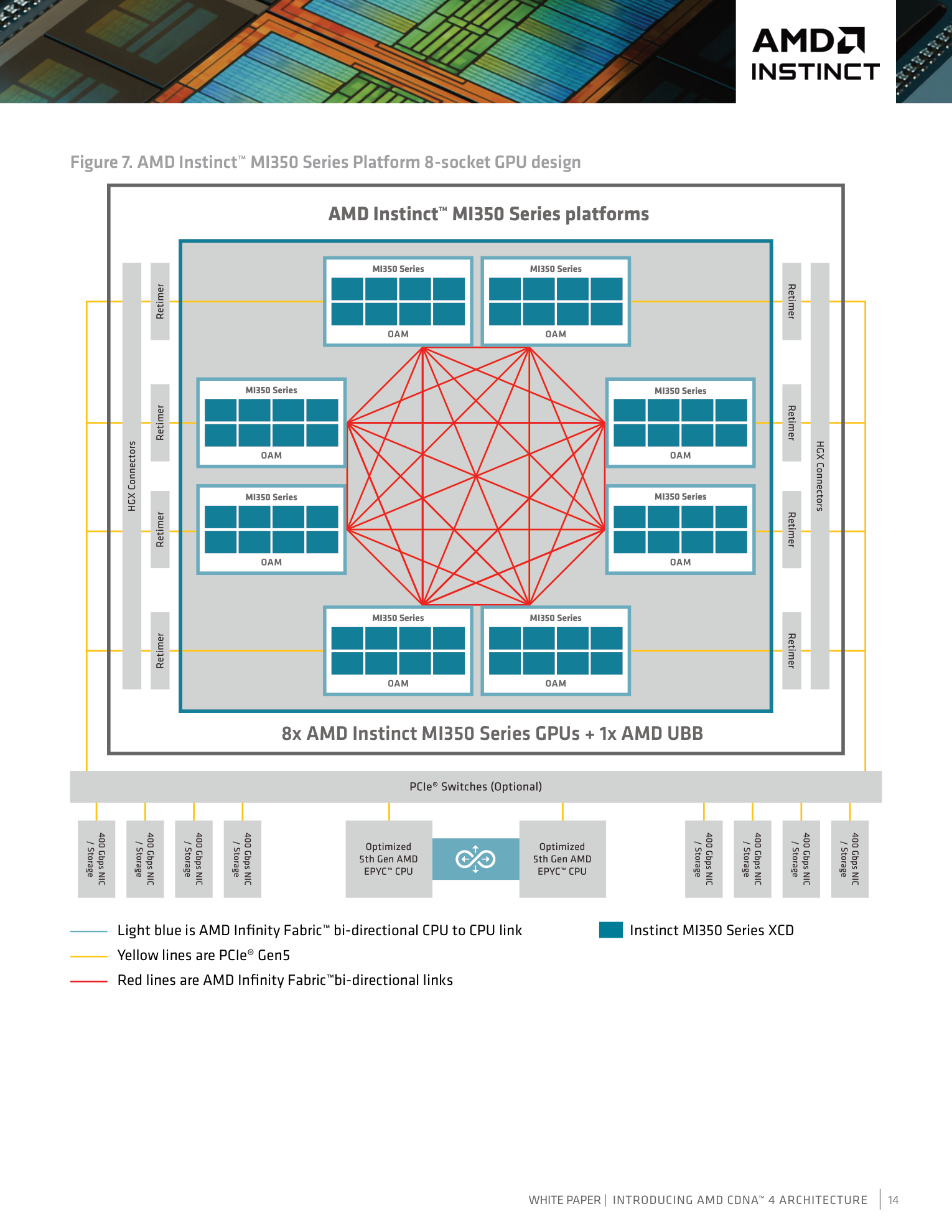
解读: 这张图展示了MI350 Series的8-GPU全互联系统拓扑,使用UBB8(Universal Base Board 8)底板。8个GPU通过Infinity Fabric链路实现全连接(all-to-all)——每个GPU使用7条IF链路分别连接其他7个GPU(每对GPU之间1条链路),剩余1条IF链路复用为PCIe Gen5连接host CPU。红色线条表示GPU间的Infinity Fabric双向链路,黄色线条表示PCIe Gen5链路,浅蓝色线条表示CPU间互联。这种全连接拓扑对于AllReduce等集合通信操作非常高效——任意两个GPU之间只需1跳。
System-level topology: Logically identical to CDNA 3 MI300X/MI325X platforms. This is deliberate for drop-in compatibility — the MI350X UBB8 baseboard is physically interchangeable with MI325X designs.
| Topology Metric | Value |
|---|---|
| Node topology | Fully connected 8-GPU (all-to-all) |
| Links per GPU pair | 1 IF link (153.6 GB/s bidir) |
| P2P aggregate per GPU | 1,075.2 GB/s (7 links) |
| Bisection BW (8 GPUs) | \(4 \times 153.6 = 614.4\ \text{GB/s}\) |
| Host link | 1× PCIe Gen5 x16 (128 GB/s) |
6c. In-Package Interconnect #
| Metric | Value |
|---|---|
| IOD-IOD bisection BW | 5.5 TB/s |
| IOD-IOD improvement vs CDNA3 | ~14% faster |
| XCD-IOD connection | 3D vertical stacking (direct through-silicon) |
The IOD simplification from 4→2 means the in-package Infinity Fabric network has fewer hops. In CDNA 3 with 4 IODs, accessing a remote IOD could require traversing through an intermediate IOD. In CDNA 4, every XCD is directly on top of one of two IODs, and the two IODs have a single direct connection. Maximum hop count for any CU to any HBM stack: XCD→local IOD (0 hops) or XCD→local IOD→remote IOD (1 hop).
6d. Scale-Out #
The whitepaper does not specify a proprietary GPU-to-GPU switch fabric (no equivalent to NVSwitch or NVL72). Multi-node scaling relies on standard networking:
- InfiniBand or Ethernet NICs attached via PCIe Gen5
- RDMA support through standard network stacks
- No proprietary AMD IF switch announced for CDNA 4
This is the most significant competitive gap vs NVIDIA Blackwell: NVLink5 provides 1,800 GB/s per GPU (vs 1,075 GB/s for IF), and NVL72 creates a 72-GPU NVLink domain with 130 TB/s aggregate — a fundamentally different scale-up capability.
7. Power, Thermal & Efficiency #
| Parameter | MI350X | MI355X |
|---|---|---|
| TDP / Max Board Power | 1,000W | 1,400W |
| Cooling | Passive (air-cooled) | Direct Liquid Cooled (DLC) |
| Form Factor | OAM (UBB8, 4RU tray) | OAM (UBB8, 2RU tray) |
| MI325X Compatible | Drop-in replacement | Requires higher power/cooling accommodation |
7a. Efficiency Metrics #
| Metric | MI350X (1000W) | MI355X (1400W) | MI300X (750W, ref) |
|---|---|---|---|
| FP16 Matrix TFLOPS/W | 2.31 | 1.80 | 1.74 |
| FP8 Matrix TFLOPS/W | 4.61 | 3.60 | 3.49 |
| MXFP4 TFLOPS/W | 9.23 | 7.19 | N/A |
| FP64 Vector TFLOPS/W | 0.072 | 0.056 | 0.109 |
| GB HBM / W | 0.288 | 0.206 | 0.256 |
Analysis:
- MI350X is more power-efficient than MI355X on every metric — the additional 400W of MI355X goes primarily to higher clock (\(2.2 \to 2.4\ \text{GHz}\), \(+9.1\%\)), yielding only \(\sim 8.7\%\) more performance. The power-performance curve is deeply into diminishing returns at 1,400W.
- vs CDNA 3 MI300X: FP8 TFLOPS/W improves from \(3.49\) to \(4.61\ (+32\%)\) for MI350X, driven by the N3P process efficiency gains. But FP64 efficiency drops due to Matrix FP64 halving.
- Rack-level impact: A 120–130 kW rack fits \(8\times\) MI350X servers (64 GPUs) \(= 0.59\ \text{EF}\) FP8 with sparsity. A 200 kW rack fits \(16\times\) MI355X servers (128 GPUs) \(= 1.28\ \text{EF}\) FP8 with sparsity — \(118\%\) more compute in comparable footprint thanks to liquid cooling density.
7b. Power Budget Breakdown (estimated) #
The whitepaper does not provide a detailed power breakdown, but based on architectural analysis:
- HBM3E (8 stacks, 8 Gbps): ~150-200W (estimated from HBM3E power density)
- XCD compute (8 XCDs at N3P): ~400-600W at 2.4 GHz
- IOD (2 IODs, Infinity Cache 256MB, IF links): ~150-250W
- IF links (7× external): ~50-100W
- Overhead (VRMs, PHYs, misc): ~100-200W
8. Software & ISA Impact #
8a. ISA Changes (gfx950 vs gfx942) #
New instructions:
| Category | Instructions | Purpose |
|---|---|---|
| Matrix (MFMA) | New MXFP8 MFMA opcodes | Matrix multiply with MXFP8 operands (shared exponent blocks) |
| Matrix (MFMA) | New MXFP6 MFMA opcodes | Matrix multiply with MXFP6 (E3M2/E2M3) operands |
| Matrix (MFMA) | New MXFP4 MFMA opcodes | Matrix multiply with MXFP4 (E2M1) operands |
| Data conversion | MX format encode/decode | Convert between FP16/BF16 and MXFP formats (pack/unpack shared exponents) |
| LDS | Direct load from L1 to LDS | Bypass VGPR staging for LDS population |
Removed/deprecated:
| Instruction | Status | Impact |
|---|---|---|
| TF32 MFMA | Removed from hardware | Must use BF16 MFMA as emulation path. Software: TF32_op ≈ BF16_MFMA(cast_to_BF16(FP32_input)) |
| FP64 MFMA (full rate) | Halved throughput | Same opcode but runs at \(128\ \text{FLOPS/clk/CU}\) vs \(256\); existing FP64 MFMA kernels work but run \(2\times\) slower per CU |
8b. Compiler & Software Stack Impact #
SDK: ROCm (open-source), Day 0 support for MI350 Series.
Framework support:
- Training: PyTorch (ROCm), JAX (ROCm), Megatron-LM, Torchtitan, Maxtext, Torchtune
- Inference: vLLM (bi-weekly stable releases), SGLang (weekly stable releases)
- Kernel optimization: Triton language, Composable Kernel (CK), MIOpen
- Orchestration: Kubernetes + AMD GPU Operator
Kernel optimization implications of CDNA 4:
- MX format quantization: Framework-level support needed to quantize model weights to MXFP6/MXFP4 and emit the correct MFMA instructions. This requires new quantization schemes (per-32-element scaling vs per-tensor).
- Tile size re-tuning: LDS 160 KB enables larger GEMM tiles — e.g., \(256 \times 128\) or \(128 \times 256\) FP16 tiles that were impossible with 64 KB LDS. Auto-tuners (Triton, CK) need updated search spaces.
- LDS direct load: Kernels can be restructured to load data L1→LDS without staging in VGPRs, freeing registers for higher occupancy.
- Occupancy changes: Fewer CUs (256 vs 304) but higher per-CU resources. Occupancy tuning may favor fewer, larger wavefronts over many smaller ones.
- Transcendental-limited kernels: Attention/softmax kernels that were transcendental-bottlenecked now have \(2\times\) headroom.
- Wavefront size: 64 work-items (unchanged from CDNA 3)
- Workgroup max: unchanged
- LDS per workgroup: up to 160 KB (was 64 KB) — enables larger workgroup sizes for data-sharing-heavy kernels
- VGPR: 512 × 32-bit per CU (shared among waves)
- AGPR: 512 × 32-bit per CU (accumulator registers for MFMA)
- Large GEMMs (M,N,K > 2048): compute-bound → will see close to \(1.93\times\) actual speedup at FP8
- Medium GEMMs (512 < M < 2048): may transition from compute-bound to memory-bound at FP8 (Ops:Byte = 629 is very high)
- MXFP6 is the GEMM sweet spot: achieves 10 PF (same as MXFP4) with better numerical accuracy (E3M2 vs E2M1). For weight matrices that tolerate 6-bit quantization (most LLM linear layers), MXFP6 delivers the optimal accuracy-performance trade-off.
- LDS 160 KB enables larger tiles: A \(256 \times 128\) BF16 tile pair occupies 128 KB, leaving 32 KB for metadata. This was impossible in CDNA 3 (64 KB LDS). Larger tiles → higher arithmetic intensity → closer to peak.
- 2× transcendental rate: softmax(QK^T) requires exp() and reciprocal operations. In CDNA 3, transcendental throughput was a bottleneck when Matrix Core rate was high. CDNA 4 doubles the SFU rate, restoring balance.
- 160 KB LDS: FlashAttention tiles Q, K, V blocks in LDS. With 160 KB, the attention tile can be much larger — e.g., holding a full \(128 \times 128\) attention block plus intermediate softmax state, reducing the number of outer loop iterations.
- LDS direct load: Q/K/V blocks can stream from L1 to LDS without VGPR staging, reducing instruction count and latency.
- 288 GB HBM3E: Critical for MoE models where each expert adds parameters. A 16-expert MoE with 70B parameters per expert could require ~140 GB in FP8 — fits in single GPU with room for KV-cache.
- 8 GPU fully connected topology: Expert parallelism requires All-to-All communication between GPUs. 1,075 GB/s P2P bandwidth enables efficient expert routing within a node.
- MXFP4 quantization: Aggressively quantizing expert weights to MXFP4 reduces memory footprint by \(2\times\) vs FP8, enabling more experts per GPU. With 10 PF MXFP4 throughput, the compute cost is zero compared to FP8.
- 288 GB capacity → larger models per GPU, longer context windows
- MXFP4/MXFP6 → aggressive weight quantization for inference
- Compute partitioning (CPX mode: 8 partitions of 36 GB each) → multi-tenant inference serving
- vLLM/SGLang Day 0 optimization
- FP8 at 5.0 PF (\(1.93\times\) vs MI325X) → faster forward/backward passes
- FP16/BF16 at 2.5 PF → strong for mixed-precision training
- LDS 160 KB → larger tiles in GEMM kernels used during training
- FP64 Matrix halved → scientific computing workloads that rely on FP64 MFMA see regression
- CU count reduction → fine-grained FP64 vector workloads slightly slower (\(\sim 0.96\times\))
- Compute parity at FP8/FP16: The raw TOPS race is effectively tied at ~5 PF FP8. Neither vendor has a meaningful compute throughput advantage for standard AI workloads.
- AMD's memory moat: 288 GB vs 192 GB (+50%) is AMD's strongest differentiator. For LLM inference, memory capacity directly determines max model size and context length per GPU. A Llama-405B in FP8 requires ~405 GB — 2 MI355X GPUs vs 3 B200 GPUs.
- NVIDIA's interconnect moat: NVLink5 (1.8 TB/s) + NVL72 (72-GPU domain) is AMD's biggest weakness. For large-scale distributed training with tensor/pipeline/expert parallelism, the interconnect gap translates to significant real-world performance differences.
- MXFP6 as differentiator: AMD's exclusive MXFP6 format achieves the same throughput as MXFP4 with better accuracy — a genuinely useful intermediate precision for weight quantization. NVIDIA has no equivalent.
- Power disadvantage: MI355X at 1,400W vs B200 at 1,000W means 40% more power per GPU. At scale, this impacts TCO significantly and requires liquid cooling infrastructure.
8c. Programming Model #
9. AI Workload Impact Analysis #
9a. GEMM (Matrix Multiplication) #
Theoretical improvement: \(1.93\times\) at FP8, \(3.85\times\) at MXFP4 (vs MI325X FP8).
Practical implications:
9b. Attention (Self-Attention / FlashAttention) #
Key hardware improvements:
Attention remains memory-bound for decode: Even with 8 TB/s HBM bandwidth, KV-cache reads for long sequences dominate decode latency. The 288 GB capacity helps by fitting larger KV-caches in a single GPU.
9c. MoE (Mixture of Experts) #
9d. Training vs Inference #
Primarily benefits inference:
Also benefits training:
Weakened for HPC training:
10. Competitive Positioning — MI355X vs NVIDIA B200 #
| Metric | AMD MI355X | NVIDIA B200 (est.) | Advantage |
|---|---|---|---|
| Process | N3P (XCD) + N6 (IOD) | TSMC 4NP | AMD (XCD node) |
| Packaging | 8 XCD + 2 IOD (3D chiplet) | Dual-die (NV-HBI 10 TB/s) | Different approaches |
| Transistors | 185B | 208B | NVIDIA |
| FP64 Matrix | 78.6 TF | ~90 TF (est.) | NVIDIA |
| FP32 Matrix | 157.3 TF | ~90 TF (est.) | AMD |
| FP16/BF16 Matrix | 2,516 TF (5,033 sparse) | ~2,500 TF (~5,000 sparse) | Parity |
| FP8 Matrix | 5,033 TF (10,066 sparse) | ~5,000 TF (~10,000 sparse) | Parity |
| MXFP6 | 10,066 TF | N/A | AMD exclusive |
| MXFP4 / FP4 | 10,066 TF | ~10,000 TF | Parity |
| HBM Capacity | 288 GB HBM3E | 192 GB HBM3E | AMD +50% |
| HBM Bandwidth | 8.0 TB/s | 8.0 TB/s | Parity |
| Interconnect BW | 1,075 GB/s (IF) | 1,800 GB/s (NVLink5) | NVIDIA +67% |
| GPU Domain Scale | 8 GPUs (all-to-all) | 72 GPUs (NVL72) | NVIDIA 9× |
| TDP | 1,400W | 1,000W | NVIDIA (lower power) |
| FP8 TFLOPS/W | 3.60 | ~5.00 | NVIDIA +39% |
| L2 + LLC | \(32 + 256 = 288\ \text{MB}\) | ~100 MB (est.) | AMD 2.9× |
| MX Format Standard | OCP MX (MXFP8/6/4) | Proprietary FP4 + micro-tensor scaling | AMD more standardized |
| Transformer Engine | Software-managed precision | Hardware TE (2nd gen) | NVIDIA |
Strategic assessment:
11. Comprehensive Spec Sheet #
| Category | Parameter | MI350X | MI355X |
|---|---|---|---|
| Architecture | Architecture | AMD CDNA 4 | AMD CDNA 4 |
| ISA Code | gfx950 | gfx950 | |
| XCD Process | TSMC N3P | TSMC N3P | |
| IOD Process | TSMC N6 | TSMC N6 | |
| Transistors | 185 Billion | 185 Billion | |
| XCDs | 8 | 8 | |
| IODs | 2 | 2 | |
| Compute | Compute Units | 256 | 256 |
| Stream Processors | 16,384 | 16,384 | |
| Matrix Cores | 1,024 | 1,024 | |
| Max Engine Clock | 2,200 MHz | 2,400 MHz | |
| Performance | FP64 Vector | 72.1 TF | 78.6 TF |
| FP32 Vector | 144.2 TF | 157.3 TF | |
| FP16 Vector | 144.2 TF | 157.3 TF | |
| FP64 Matrix | 72.1 TF | 78.6 TF | |
| FP32 Matrix | 144.2 TF | 157.3 TF | |
| FP16 Matrix / Sparse | 2.3 PF / 4.6 PF | 2.5 PF / 5.0 PF | |
| BF16 Matrix / Sparse | 2.3 PF / 4.6 PF | 2.5 PF / 5.0 PF | |
| FP8 (OCP) Matrix | 4.6 PF | 5.0 PF | |
| MXFP8 Matrix | 4.6 PF | 5.0 PF | |
| MXFP6 / MXFP4 Matrix | 9.2 PF | 10 PF | |
| INT8 / INT8 Sparse | 4.6 POPs / 9.2 POPs | 5.0 POPs / 10 POPs | |
| Memory | Type | HBM3E | HBM3E |
| Capacity | 288 GB | 288 GB | |
| Interface | 1024b × 8 stacks | 1024b × 8 stacks | |
| Bandwidth | up to 8.0 TB/s | up to 8.0 TB/s | |
| Cache | L1 Data | 32 KB/CU | 32 KB/CU |
| LDS | 160 KB/CU | 160 KB/CU | |
| L2 | 4 MB/XCD (32 MB total) | 4 MB/XCD (32 MB total) | |
| Infinity Cache | 256 MB | 256 MB | |
| Interconnect | IF Links | 7×16 + 1× PCIe Gen5 | 7×16 + 1× PCIe Gen5 |
| P2P Ring BW (8 GPUs) | 1,075.2 GB/s | 1,075.2 GB/s | |
| Total Aggregate IO BW | 1,203.2 GB/s | 1,203.2 GB/s | |
| Host | PCIe Gen 5 x16 | PCIe Gen 5 x16 | |
| Virtualization | SR-IOV | Yes | Yes |
| Max Partitions | 8 (CPX) | 8 (CPX) | |
| Video Decode | 4 groups (HEVC/H.264/VP9/AV1) | 4 groups | |
| RAS | Full-Chip ECC | Yes | Yes |
| Page Retirement | Yes | Yes | |
| Page Avoidance | Yes | Yes | |
| Board | Form Factor | OAM | OAM |
| Thermal | Passive (air) | Liquid (DLC) | |
| Max Power | 1,000W | 1,400W | |
| Tray Height | 4RU | 2RU | |
| MI325X Compatible | Drop-in | Needs power/cooling upgrade |
12. Infrastructure Impact #
| Layer | Impact |
|---|---|
| Algorithm | MXFP6 creates a new quantization tier between FP8 and FP4 — algorithm researchers need to develop and validate per-block microscaling quantization recipes (32-element granularity). The shared exponent mechanism means outlier-sensitive layers (attention Q/K) may need MXFP8, while FFN weights can use MXFP6/MXFP4. Dynamic precision selection (akin to NVIDIA's Transformer Engine but software-driven) becomes essential. |
| Kernel | LDS 160 KB + 256 B/clk enables fundamentally larger GEMM tiles (e.g., \(256 \times 128\) FP16) that were impossible on CDNA 3. Kernel auto-tuners (Triton, CK) must expand search space. L1→LDS direct load changes the optimal data staging pattern — VGPR-bypass kernels need rewriting. 2× transcendental rate means attention kernels should rebalance softmax vs MFMA pipeline to maintain throughput. |
| Framework | PyTorch/JAX need native MX format tensors with per-block scaling metadata. Quantization toolchains (GPTQ, AWQ, SmoothQuant) need MXFP6/MXFP4 backends. The BF16 TF32 emulation path needs framework-level routing so existing TF32 codepaths gracefully fallback. |
| LLM | 288 GB enables single-GPU serving of ~400B parameter FP8 models (or ~800B in MXFP4). 10 PF MXFP4 throughput makes 70B-class model inference at sub-10ms TTFT feasible. Context window scaling: 288 GB - model_weights leaves substantial KV-cache headroom for 128K+ token contexts. MoE models benefit most: more experts fit per GPU at MXFP4 precision. |
| Agent | Real-time agentic inference benefits from MXFP4's 10 PF throughput and 288 GB capacity — a single MI355X can serve multiple concurrent agent sessions with large context windows. The 8-way compute partitioning (CPX mode, 36 GB/partition) enables efficient multi-tenant agent serving on a single GPU. |
| Cluster | 8-GPU fully connected topology is unchanged from CDNA 3 — existing cluster software works. But the lack of an NVL72-equivalent limits scale-up beyond 8 GPUs to standard networking (InfiniBand/Ethernet). Cluster architects must compensate with network-level optimizations (NCCL-compatible collectives over RDMA). The 20% IF bandwidth increase (1,075 vs 896 GB/s) helps within-node but does not address the cross-node gap vs NVLink Switch fabrics. Power infrastructure must handle \(1{,}400\ \text{W/GPU} \times 8 = 11.2\ \text{kW}\) per server for MI355X nodes. |