NVIDIA A100 Tensor Core GPU Architecture White Paper
NVIDIA A100 Tensor Core GPU Architecture White Paper #
NVIDIA | 2020-05 | https://images.nvidia.com/aem-dam/en-zz/Solutions/data-center/nvidia-ampere-architecture-whitepaper.pdf Category: hardware | Tags: gpu-architecture, tensor-core, a100, ampere, mig, sparsity, tf32 Read: 2026-04-16
Core Contribution #
第三代Tensor Core支持全数据类型(含FP64 TC和TF32),引入MIG多实例GPU和2:4结构化稀疏,奠定数据中心GPU标准。
Summary #
A100基于TSMC 7nm工艺,die面积826mm²,集成54.2B晶体管,配备108个SM、6,912个CUDA Cores和432个第三代Tensor Core。核心创新包括:(1) TF32——一种19-bit浮点格式(8-bit exponent + 10-bit mantissa),兼容FP32输入却能在Tensor Core上以8x FP32的速度运算,使现有FP32 DL模型无需代码修改即可获得10x V100 FP32的加速;(2) FP64 Tensor Core——首次将矩阵加速扩展到双精度浮点,为HPC科学计算(如分子动力学、气候模拟)提供19.5 TFLOPS的FP64矩阵吞吐,达V100 FP64的2.5倍;(3) 2:4结构化稀疏——硬件原生支持细粒度稀疏模式(每4个权重中2个为零),Tensor Core吞吐直接翻倍而精度损失极小。
显存子系统方面,A100配备80GB HBM2e显存(带宽2,039 GB/s),L2 Cache从V100的6MB大幅扩展至40MB(6.7x),配合L2 Residency Control可将热点数据钉在L2中,显著降低HBM访问次数。每SM拥有192KB的可配置Shared Memory/L1(V100为128KB,1.5x提升),支持更大的tile size以提升TC利用率。互联方面采用第三代NVLink,12条链路共600GB/s(V100的2倍),支持8-GPU全互联DGX A100系统。
MIG(Multi-Instance GPU)是A100的革命性特性——可将单颗GPU硬件级隔离为最多7个独立实例,每个实例拥有独立的SM、L2 Cache切片、显存控制器和显存容量,实现QoS保证和安全隔离。这使数据中心能在同一GPU上混合运行不同规模的推理任务和小规模训练任务,大幅提升GPU利用率。
Key Findings #
- 108 SM, 6,912 CUDA Cores (64 FP32/SM), 432 Tensor Cores (4/SM, 3rd gen)
- TF32 TC: 156 TFLOPS (312 TFLOPS with 2:4 sparsity),无需代码修改即可加速FP32 DL workload
- FP64 TC: 19.5 TFLOPS (2.5x V100 FP64)——首次Tensor Core支持双精度
- FP16/BF16 TC: 312 TFLOPS (624 sparse),2.5x V100 FP16 TC
- INT8 TC: 624 TOPS (1,248 sparse);INT4 TC: 1,248 TOPS (2,496 sparse)
- 2:4 Structured Sparsity: 硬件原生支持,所有TC数据类型吞吐翻倍
- 80GB HBM2e, 2,039 GB/s (2.27x V100)
- 40MB L2 Cache (6.7x V100的6MB),支持L2 Residency Control
- 192KB Shared Memory/L1 per SM (1.5x V100的128KB)
- MIG: 最多7个GPU Instance,硬件级隔离(SM、L2、显存独立)
- NVLink 3: 12 links, 600GB/s total (2x V100)
- PCIe Gen 4 x16
- TDP: 400W (SXM4)
- Async Copy: 直接从Global Memory到Shared Memory,绕过RF
- 全芯片(GA100): 8 GPCs, 128 SMs, 512 TCs——A100产品启用108 SMs
Key Tables #
Table 1: A100 Performance Specs (All Data Types) #
| Data Type | Tensor Core | Tensor Core + Sparsity | CUDA Core |
|---|---|---|---|
| FP64 | 19.5 TFLOPS | — | 9.7 TFLOPS |
| TF32 | 156 TFLOPS | 312 TFLOPS | — |
| FP32 | — | — | 19.5 TFLOPS |
| BF16 | 312 TFLOPS | 624 TFLOPS | — |
| FP16 | 312 TFLOPS | 624 TFLOPS | — |
| INT8 | 624 TOPS | 1,248 TOPS | — |
| INT4 | 1,248 TOPS | 2,496 TOPS | — |
Table 2: A100 vs V100 Comparison #
| Metric | V100 SXM2 | A100 SXM4 (80GB) | Speedup |
|---|---|---|---|
| Process | 12nm | 7nm | — |
| Die Size | 815 mm² | 826 mm² | — |
| Transistors | 21.1B | 54.2B | 2.6x |
| SMs | 80 | 108 | 1.35x |
| CUDA Cores | 5,120 | 6,912 | 1.35x |
| Tensor Cores | 640 (1st gen) | 432 (3rd gen) | redesigned |
| FP64 | 7.8 TF | 9.7 TF | 1.24x |
| FP64 TC | — | 19.5 TF | new |
| FP32 | 15.7 TF | 19.5 TF | 1.24x |
| TF32 TC | — | 156 TF | new (10x V100 FP32) |
| FP16 TC | 125 TF | 312 TF | 2.5x |
| FP16 TC sparse | — | 624 TF | 5x V100 FP16 TC |
| Memory | 32 GB HBM2 | 80 GB HBM2e | 2.5x |
| Bandwidth | 900 GB/s | 2,039 GB/s | 2.27x |
| L2 Cache | 6 MB | 40 MB | 6.7x |
| Shared/L1 per SM | 128 KB | 192 KB | 1.5x |
| NVLink BW | 300 GB/s | 600 GB/s | 2x |
| MIG | — | 7 instances | new |
| TDP | 300W | 400W | +33% |
Table 3: MIG Partitioning Options #
| GPU Instance | SMs | Memory | Use Case |
|---|---|---|---|
| 1x Full | 108 | 80 GB | Large training |
| 2x Half | 54 each | 40 GB each | Medium workloads |
| 3x ~1/3 | 36 each | ~26 GB each | Mixed inference |
| 7x Slice | ~14 each | ~10 GB each | Small inference |
Limitations #
- MIG的7-instance上限和固定分区粒度限制了灵活性,不支持任意比例划分
- 2:4 Sparsity要求严格的结构化模式(每4元素恰好2个零),并非所有模型/层都能轻松满足
- INT4 TC虽有吞吐但实际AI模型很少使用INT4量化(精度损失大)
- 单die设计(826mm²)接近光刻极限,良率压力大
- 80GB显存在大型LLM推理场景逐渐显得不足(GPT-3 175B需多卡)
- FP64 TC虽然是突破,但19.5 TFLOPS仍低于AMD MI250X的95.7 TFLOPS FP64 Matrix
- NVLink 600GB/s对于AllReduce密集型大规模训练仍是瓶颈
Infrastructure Impact #
- 奠定数据中心GPU标准: A100定义了"AI加速器"的完整功能集——TC全精度覆盖、结构化稀疏、多实例隔离、大L2 Cache
- MIG改变部署模式: 允许云厂商在同一GPU上提供不同大小的虚拟GPU实例,直接影响AWS/Azure/GCP的GPU实例产品线
- TF32降低迁移门槛: 现有FP32训练代码无需修改即可获得显著加速,加速了从CPU到GPU的workload迁移
- DGX A100系统: 8x A100 + 6x NVSwitch构成5 PFLOPS AI系统,成为AI训练的"标准单元"
- 推动MLPerf基准: A100在MLPerf Training/Inference多项benchmark中长期霸榜
- 2:4 Sparsity推动模型压缩研究: 催生了大量结构化剪枝算法研究
Deep Analysis (hardware) #
1. Architecture Overview & Naming #
- 产品名称: NVIDIA A100 Tensor Core GPU
- GPU代号: GA100
- 架构名: NVIDIA Ampere (第8代数据中心GPU)
- 工艺节点: TSMC 7nm N7 FinFET
- Die面积: 826 mm²
- 晶体管数: 54.2 billion
- 封装方式: Monolithic die (单一大芯片,非chiplet)
- 目标市场: 数据中心AI训练/推理、HPC科学计算、数据分析
- 产品形态: SXM4 (400W, NVLink), PCIe (250W)
Full GA100 die包含8 GPCs, 8 TPCs/GPC, 2 SMs/TPC = 128 SMs total, 512 Tensor Cores, 8,192 FP32 CUDA Cores。内存子系统: 6 HBM2 stacks, 12 × 512-bit memory controllers。A100产品因良率优化禁用部分单元: 7 GPCs + 1 partial = 108 SMs (84.4% utilization), 432 TCs, 6,912 CUDA Cores; 5 HBM2 stacks, 10 × 512-bit controllers。
Figure 1: GA100 Full GPU Block Diagram #
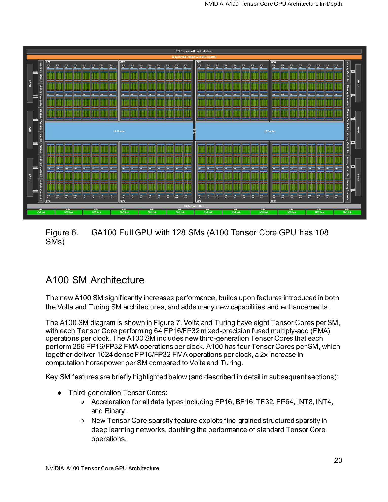
解读: GA100全芯片架构图展示完整的8 GPC布局,每GPC内含8个TPC(每TPC 2个SM),共128个SM。图中GPC围绕中央L2 Cache(40MB in product)对称排列,上下两侧为HBM2 memory controller和HBM stack接口。NVLink 3.0的12条链路分布在die两侧边缘,PCIe Gen 4接口位于die底部。整体布局体现GPC→TPC→SM三级层次结构——这一拓扑从Volta延续至今。A100产品禁用20个SM(128→108)用于良率优化,这是826mm²大die在7nm节点的必要妥协。图中每个GPC内部可见8个TPC单元(蓝色方块),每TPC内含2个SM,以及GPC级别的Raster Engine和ROP(graphics单元在数据中心SKU中不活跃)。
2. Generational Delta (A100 Ampere vs V100 Volta) #
2a. 新增单元 (Added) #
| New Unit / Feature | Description | Why it matters for AI |
|---|---|---|
| TF32 Tensor Core Mode | 19-bit格式(8-bit exp + 10-bit mantissa + sign),TC自动截断FP32输入为TF32 | 零代码修改加速FP32 DL训练,10x V100 FP32吞吐 |
| FP64 Tensor Core | 首次TC支持IEEE FP64矩阵乘加 | HPC科学计算(分子动力学、CFD)获得2.5x FP64加速 |
| BF16 Tensor Core | TC支持BF16输入/FP32累加,与FP16同吞吐 | BF16更大动态范围减少loss scaling需求 |
| 2:4 Structured Sparsity | 硬件原生fine-grained稀疏:每4连续元素恰好2零 | 所有TC数据类型吞吐自动翻倍(需配合剪枝训练) |
| MIG (Multi-Instance GPU) | 硬件级GPU分区,最多7独立实例 | 云端多租户推理,提升GPU利用率+QoS保证 |
| Async Copy (Global→Shared) | 新指令直接从Global Memory搬到Shared Memory | 绕过Register File,减少RF带宽和功耗 |
| Async Barrier | Shared memory中的硬件加速屏障 | 与Async Copy配合实现compute-copy overlap |
| L2 Residency Control | cudaAccessPolicyWindow API将数据钉在L2 | 减少HBM流量,working set < 40MB显著加速 |
| INT4 Tensor Core | TC支持INT4精度 | 极低精度推理(实际AI应用有限) |
| Compute Data Compression | L2→DRAM数据压缩 | 等效增加最多4x DRAM带宽和2x L2容量 |
2b. 删除/移除 (Removed) #
| Removed Unit / Feature | Reason | Impact |
|---|---|---|
| 独立FP16×2 CUDA Core路径 | TC已覆盖FP16矩阵运算,CUDA FP16走packed路径 | 对non-GEMM FP16操作无实质影响 |
| RT Core (光追单元) | GA100为纯计算die(GA102/消费级有RT Core) | 数据中心无需RT,die面积释放给计算和cache |
2c. 增强/升级 (Enhanced) #
| Enhanced Unit | V100 (Volta) | A100 (Ampere) | Improvement | How Measured |
|---|---|---|---|---|
| Tensor Core | 1st gen: 8/SM, 64 FP16 FMA/TC/clk | 3rd gen: 4/SM, 256 FP16 FMA/TC/clk | 2x per-SM throughput | 1024 vs 512 FP16 FMA/SM/clk |
| SM Count | 80 | 108 | 1.35x | Product-level |
| FP32 CUDA Cores | 5,120 (64/SM) | 6,912 (64/SM) | 1.35x | SM count scaling |
| L2 Cache | 6 MB | 40 MB | 6.67x | Total capacity |
| Shared/L1 per SM | 128 KB | 192 KB | 1.5x | Configurable split |
| HBM Capacity | 32 GB HBM2 | 80 GB HBM2e | 2.5x | Total GB |
| HBM Bandwidth | 900 GB/s | 2,039 GB/s | 2.27x | Peak BW |
| NVLink | 6 links, 300 GB/s | 12 links, 600 GB/s | 2x | Bidirectional |
| PCIe | Gen 3 | Gen 4 | 2x bandwidth | Per-direction |
2d. 架构级变更 #
- Tensor Core重构: V100的8个小TC(64 FMA each)合并为4个大TC(256 FMA each),减少调度开销,提升operand sharing效率。TC数量减半但每TC吞吐4x → 净2x/SM
- FP32/INT32双通路: A100保留V100的独立FP32和INT32数据通路(每sub-partition 16 FP32 + 16 INT32),可同一周期并行执行不同warp的FP32和INT32指令。FP16操作可在两条通路上packed执行 → \( \text{FP16 CUDA} = 4 \times \text{FP32} \)
- L2 Cache重构: 从V100的6MB简单L2变为40MB partitioned crossbar结构,L2读带宽2.3x V100。MIG模式下L2 slice独立分配给各GPU Instance
- Shared Memory扩展: 最大可配置164KB SMEM (V100最大96KB),支持更大GEMM tile以提升TC utilization
3. Compute Unit Deep Dive #
3a. SM Structure #
Figure 2: GA100 Streaming Multiprocessor (SM) #
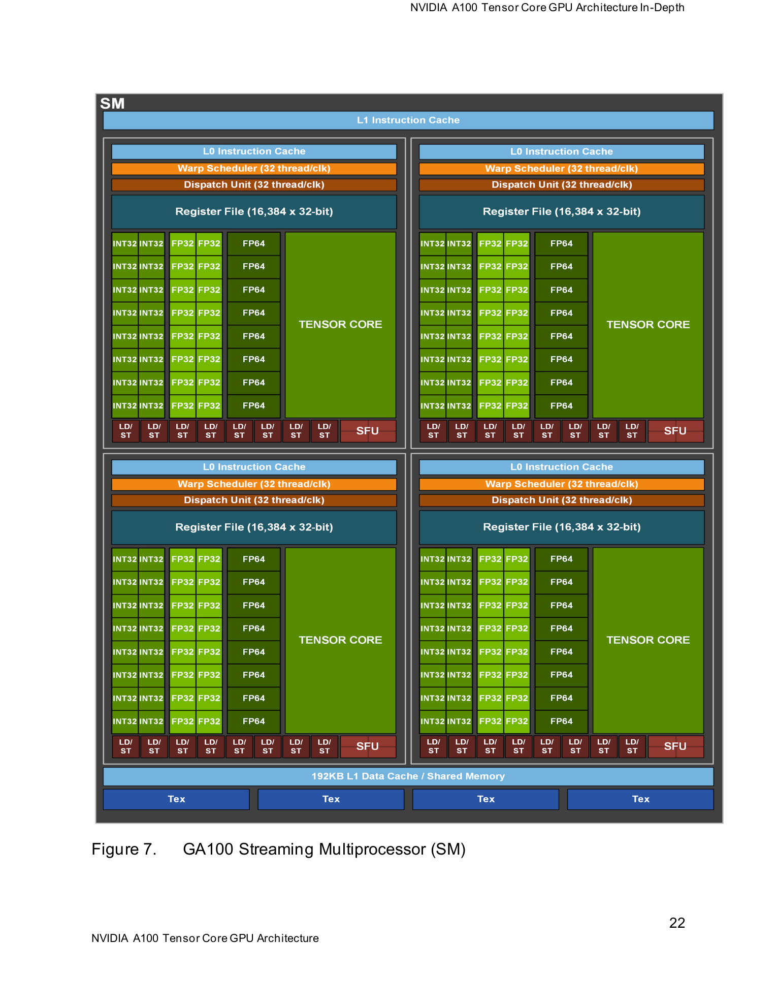
解读: GA100 SM内部架构图展示4个Processing Block(Sub-partition)的对称布局。每Block包含:16个FP32 CUDA Core、16个INT32 Core(独立数据通路,可与FP32同时执行)、1个3rd-gen Tensor Core、1个Warp Scheduler + Dispatch Unit、8个LD/ST Unit、4个SFU。图中央是192KB统一L1 Data Cache/Shared Memory(可配置分割)。Register File(256KB total = 64KB/Block)位于每Block顶部。关键变化vs V100: TC从8→4但每TC吞吐4x,L1/Shared从128→192KB,async copy路径直接Global→Shared。
SM完整配置:
| Component | Per Sub-Partition | Per SM | Notes |
|---|---|---|---|
| FP32 CUDA Cores | 16 | 64 | FP32-dedicated path |
| INT32 Cores | 16 | 64 | Independent path (also executes FP16 packed) |
| FP64 Units | 8 | 32 | Half-rate FP64 |
| 3rd Gen Tensor Core | 1 | 4 | Redesigned, 4x throughput vs V100 TC |
| Warp Scheduler | 1 | 4 | Each schedules 1 warp/cycle |
| Dispatch Unit | 1 | 4 | |
| LD/ST Units | 8 | 32 | |
| SFU | 4 | 16 | Transcendental functions |
| Register File | 64 KB (16,384 × 32-bit) | 256 KB | Same as V100 |
| Shared Memory / L1 | — | 192 KB (configurable) | 1.5x V100 |
| Max Warps | 16 | 64 | Compute Capability 8.0 |
| Max Threads | 512 | 2,048 |
数据通路特性:
- FP32通路和INT32通路完全独立,可同一周期并行执行不同warp的FP32和INT32指令
- FP16可在两条通路packed执行(每core 2 FP16 ops) → \( \text{FP16 CUDA} = 4 \times \text{FP32} = 78\ \text{TFLOPS} \)
- BF16仅在FP32通路执行(2:1 packing) → \( \text{BF16 CUDA} = 2 \times \text{FP32} = 39\ \text{TFLOPS} \)
3b. Third-Generation Tensor Core Specifications #
Figure 3: A100 vs V100 Tensor Core Operations #
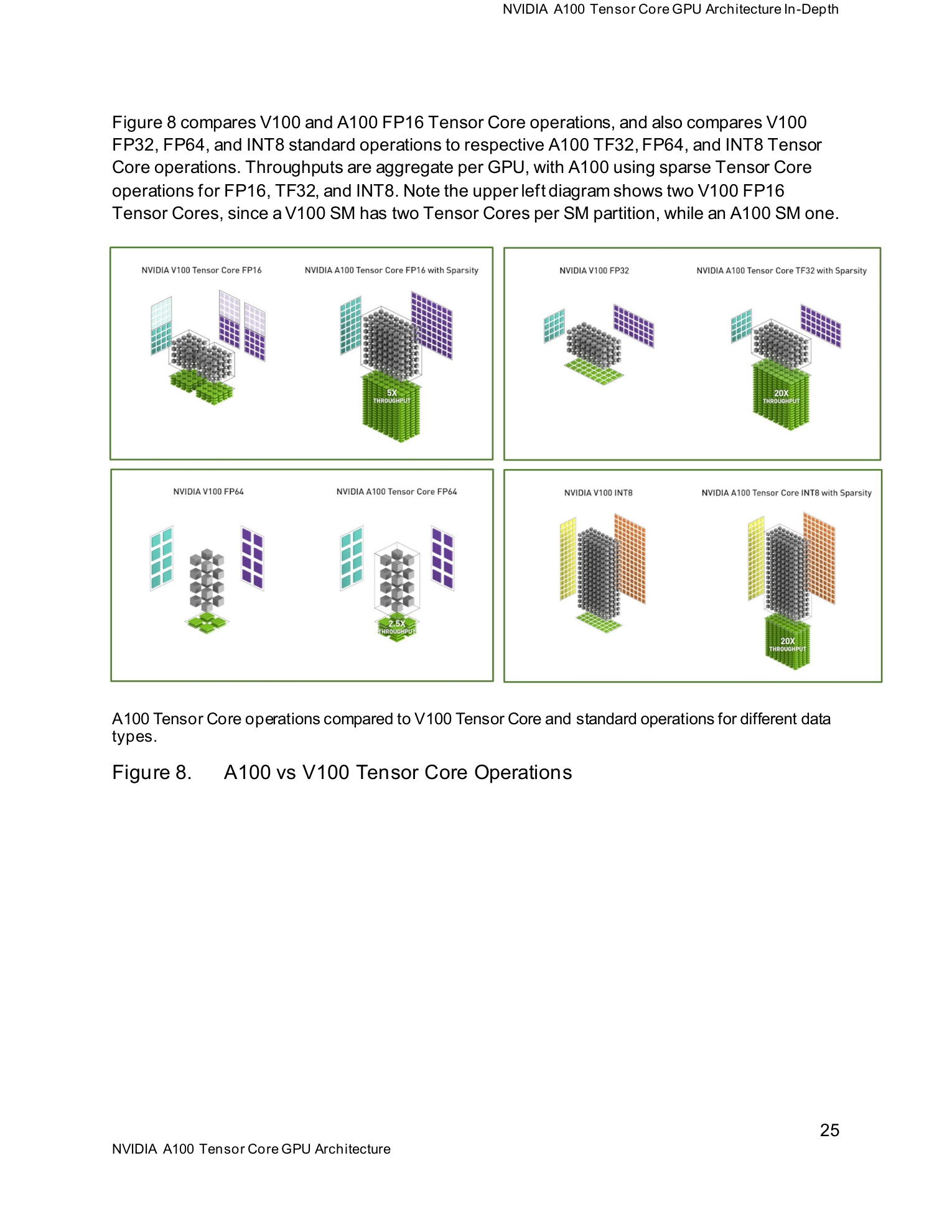
解读: V100 vs A100 Tensor Core操作对比。左上: V100每sub-partition有2个TC(共8/SM),每TC执行4×4×4 FP16 FMA(64 FMA/clk)。右上: A100每sub-partition有1个TC(共4/SM),但每TC执行等效8×4×8矩阵块(256 FP16 FMA/clk)。下排展示A100新增的TF32(10x V100 FP32)、FP64 TC(2.5x V100 FP64)、INT8 TC(10x V100 INT8)操作。关键insight: A100通过减少TC数量但大幅提升每TC吞吐,优化了operand sharing和warp scheduler效率。
| Data Type | Input | Accumulator | FMA/TC/clk | FLOPS/TC/clk | Warp MMA Shape |
|---|---|---|---|---|---|
| FP16 | FP16 | FP32/FP16 | 256 | 512 | m16n8k16 |
| BF16 | BF16 | FP32 | 256 | 512 | m16n8k16 |
| TF32 | TF32 (from FP32) | FP32 | 128 | 256 | m16n8k8 |
| FP64 | FP64 | FP64 | 16 | 32 | m8n8k4 |
| INT8 | INT8 | INT32 | 512 | 1,024 | m16n8k32 |
| INT4 | INT4 | INT32 | 1,024 | 2,048 | m16n8k64 |
| Binary | 1-bit | INT32 | 4,096 | — | m16n8k256 |
Sparsity硬件机制:
Figure 4: Fine-Grained Structured 2:4 Sparsity #
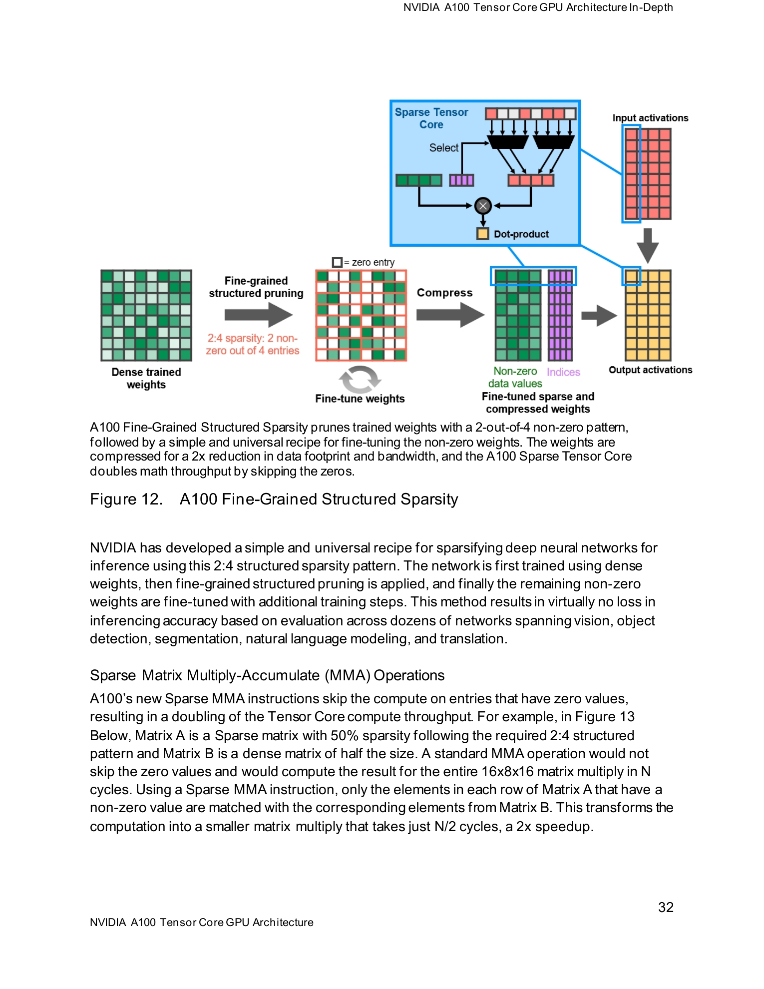
解读: 2:4结构化稀疏原理。A矩阵(weight)的每组4个连续元素中恰好2个非零(蓝色)、2个零(灰色)。硬件使用compact metadata(2-bit index per non-zero element)指示非零位置。Sparse MMA先通过metadata从B矩阵中选取对应列,再执行压缩后的矩阵乘——实际计算量减半,结果数学等价。此结构化模式比任意稀疏更易硬件实现且保证throughput deterministic。实验显示多数DNN精度损失<0.5%(whitepaper Appendix B Table 11)。
4. Peak Performance Derivation #
基准参数 (A100 SXM4 80GB):
- SM Count: 108
- Tensor Cores per SM: 4
- GPU Boost Clock: 1,410 MHz (whitepaper Table 8确认)
4a. FP32 CUDA Core Derivation #
\[
\text{FP32 Peak} = N_{\text{SM}} \times N_{\text{CUDA/SM}} \times 2 \times f_{\text{boost}} = 108 \times 64 \times 2 \times 1.41\ \text{GHz} = 19{,}491\ \text{GFLOPS} \approx 19.5\ \text{TFLOPS}\ \checkmark
\]
4b. 逐数据类型 Tensor Core 推导 #
FP16 / BF16 Tensor Core:
| Parameter | Value | Source |
|---|---|---|
| SMs | 108 | Whitepaper |
| TCs per SM | 4 | Whitepaper Fig 7 |
| FMA per TC per cycle | 256 | "256 FP16/FP32 FMA operations per clock" |
| FLOPS per TC per cycle | 512 (=256×2) | Each FMA = multiply + add |
| FLOPS per SM per cycle | 2,048 (=4×512) | Derived |
| Boost Clock | 1.41 GHz | Whitepaper Table 8 |
| Peak FP16 TC | 108 × 2,048 × 1.41 = 312 TFLOPS | ✓ matches official |
TF32 Tensor Core:
| Parameter | Value | Source |
|---|---|---|
| FMA per TC per cycle | 128 | TF32 is 19-bit → half FP16 throughput |
| FLOPS per TC per cycle | 256 | |
| Peak TF32 TC | 108 × 4 × 256 × 1.41 = 156 TFLOPS | ✓ |
FP64 Tensor Core:
| Parameter | Value | Source |
|---|---|---|
| FMA per TC per cycle | 16 | FP64 is 64-bit → 1/16 of FP16 throughput |
| FLOPS per TC per cycle | 32 | |
| Peak FP64 TC | 108 × 4 × 32 × 1.41 = 19.5 TFLOPS | ✓ |
INT8 / INT4 Tensor Core:
| Parameter | INT8 | INT4 |
|---|---|---|
| Ops per TC per cycle | 1,024 | 2,048 |
| Peak | 108 × 4 × 1,024 × 1.41 = 624 TOPS ✓ | 108 × 4 × 2,048 × 1.41 = 1,248 TOPS ✓ |
FP64 CUDA Core:
\[
\text{FP64 Peak} = 108 \times 32 \times 2 \times 1.41 = 9{,}745\ \text{GFLOPS} \approx 9.7\ \text{TFLOPS}\ \checkmark
\]
(half-rate FP64: \( 32\ \text{FP64 units/SM} = 8\ \text{per sub-partition} \))
所有推导值与官方spec完全吻合——A100的1,410 MHz boost clock对所有数据类型一致适用(不存在H100那样的TC/CUDA差异化boost)。
Figure 7: A100 Performance Specs Table #
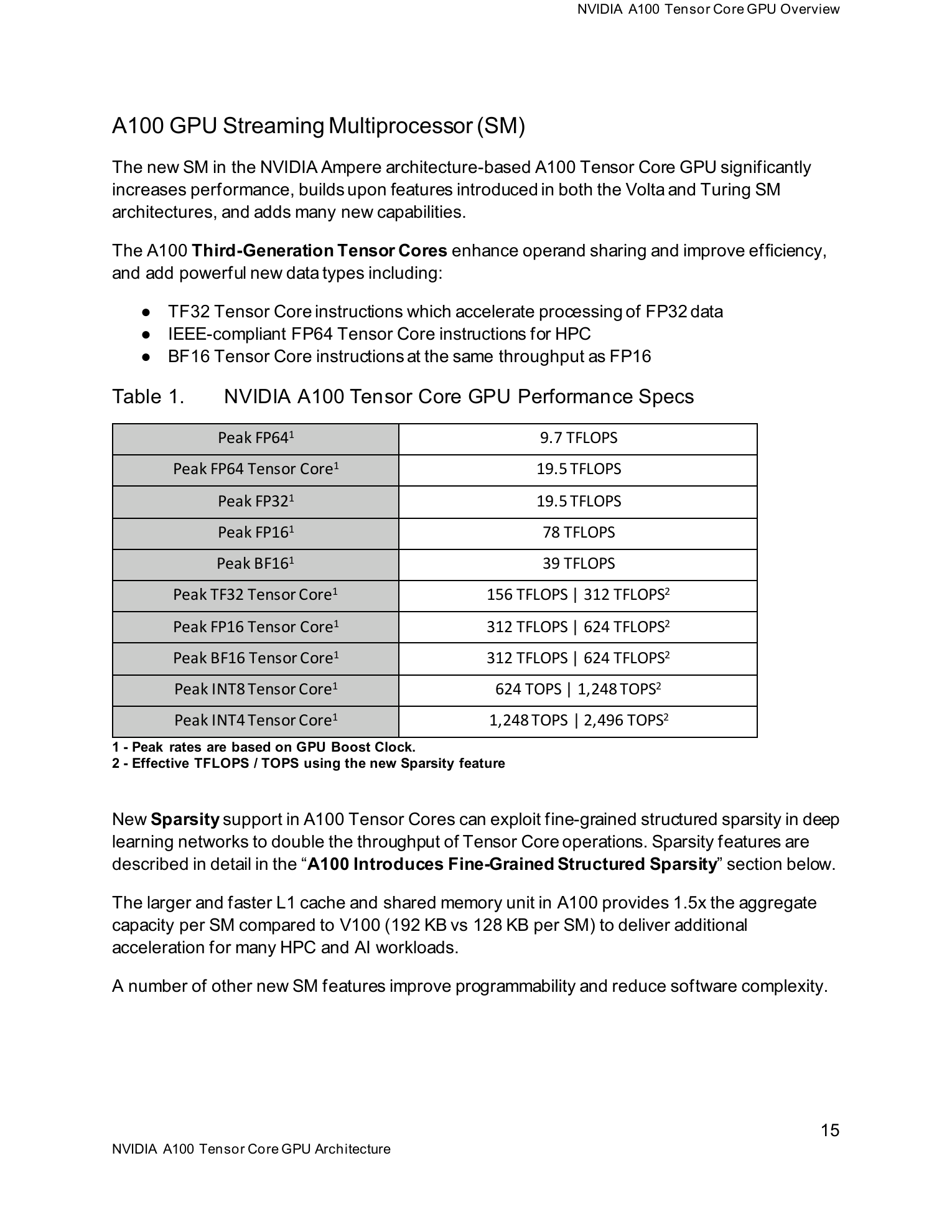
解读: 官方性能规格表,"Peak rates are based on GPU Boost Clock"(1410 MHz)。FP16 non-TC(78 TFLOPS) = 4× FP32(19.5 TFLOPS)——因FP16可在FP32和INT32两条通路packed执行。Sparsity列为所有TC数据类型翻倍。Binary TC(4,992 TOPS)为理论极限,实际无AI workload使用。
4c. Sparsity Multiplier #
2:4 Structured Sparsity翻倍TC吞吐的前提条件:
- 权重矩阵必须满足严格的2:4模式(每4个连续元素恰好2个零)
- 仅对A矩阵(weight)的K维度稀疏压缩,B矩阵(activation)保持dense
- 需通过pruning-aware training或post-training pruning获得合格稀疏模式
- 运行时使用cuSPARSELt库或CUTLASS Sparse GEMM kernel
- Partitioned Crossbar: 40MB分为多个bank/slice,每slice关联特定memory controller
- L2 Residency Control:
cudaAccessPolicyWindowAPI控制数据驻留策略(Persisting / Streaming / Normal) - MIG L2分区: 每个GPU Instance获得独立L2 slice,确保性能隔离(不同instance不会互相evict)
- Compute Data Compression: L2↔HBM传输无损压缩,等效最多4x HBM带宽和2x L2容量
- 8-GPU All-to-All via NVSwitch v2: 8× A100 + 6× NVSwitch v2
- 每颗NVSwitch: 36个NVLink 3.0端口,交换带宽7.2 Tbps
- 拓扑: Non-blocking all-to-all——任意GPU对可达600 GB/s全带宽
- 系统总算力: 8 × 312 = 2,496 TFLOPS FP16 TC (5 PFLOPS sparse)
- InfiniBand: DGX A100配备8× Mellanox ConnectX-6 HDR (200 Gbps each)
- 总节点间带宽: 8 × 200 Gbps = 1.6 Tbps = 200 GB/s
- GPUDirect RDMA: NIC直接读写GPU显存(bypass CPU)
- GPUDirect Storage: NVMe→GPU显存直通
- NVIDIA Magnum IO SDK: 优化multi-node集合通信
- MMA指令族 (Tensor Core):
mma.sync.aligned.m16n8k16.f16— FP16矩阵乘加 (替代V100的hmma.m8n8k4)mma.sync.aligned.m16n8k8.tf32— TF32矩阵乘加 (全新)mma.sync.aligned.m8n8k4.f64— FP64矩阵乘加 (全新,替代8条DFMA)mma.sync.aligned.m16n8k32.s8— INT8矩阵乘加mma.sync.aligned.m16n8k64.s4— INT4矩阵乘加- 所有MMA的
.sp后缀变体 — Sparse MMA - 异步内存指令:
cp.async.ca.shared.global— Global→Shared异步拷贝(绕过RF)cp.async.commit_group/cp.async.wait_group— 异步组管理- 屏障指令:
mbarrier.init/mbarrier.arrive/mbarrier.wait— 共享内存中的异步barrier- 归约指令:
redux.sync.{add,min,max,and,or,xor}— Warp-level归约 (Cooperative Groups)- Cache管理:
- L2 residency hint指令
- CUDA 11.0+: 支持Compute Capability 8.0
- cuBLAS: TF32模式默认开启(
CUBLAS_TF32_TENSOR_OP_MATH),FP32 GEMM自动走TC - cuDNN: 自动选择最优TC数据类型
- CUTLASS 2.x: 新增Ampere-optimized GEMM templates,支持async copy和multi-stage pipeline
- cuSPARSELt: 全新库,专用于2:4结构化稀疏GEMM
- torch.cuda.amp: AMP无缝利用FP16/BF16 TC混合精度
- Warp size: 32 (unchanged from V100)
- Max threads per block: 1,024 (unchanged)
- Max shared memory per block: 163 KB (from V100's 96 KB, +70%)
- Max registers per thread: 255 (unchanged)
- Async Copy Pipeline: 引入multi-stage pipeline概念——prefetch stage N+1数据到SMEM的同时compute stage N的数据。cp.async + mbarrier配合可实现3-4 stage软件pipeline,隐藏DRAM延迟
- MMA Shape变化: m16n8k16(FP16) vs V100的m8n8k4 → CUTLASS tile size需重新选择(从64×64到128×128+)
- 理论峰值提升: 2.5x FP16 TC / 5x with sparsity vs V100
- 实际大GEMM (M,N,K > 1024): ~2.3-2.5x (接近理论,compute-bound)
- 小GEMM (M < 512): 转为memory-bound,提升更多来自L2(6.7x)和HBM带宽(2.27x)
- TF32 GEMM: FP32模型零修改获得~8x加速 → 极大降低DL迁移门槛
- Sparsity GEMM: 剪枝后达5x V100(需cuSPARSELt)
- A100时代(2020)尚无Flash Attention(2022发表),attention kernel主要为naive实现
- 192KB SMEM: 可在shared memory中存放更大Q/K tile → 减少HBM读取
- 40MB L2: 对small-to-medium模型,部分KV Cache可驻留L2
- A100的大SMEM和L2为后来Flash Attention在A100上的高效实现奠定硬件基础
- Expert Parallelism: MIG可将不同expert放在不同GPU Instance(但粒度粗,不适合细粒度MoE)
- All-to-All: NVLink 600 GB/s为8-GPU系统的expert token routing提供充足带宽
- 显存: 80GB可容纳~16个5GB expert;大型MoE(100+ experts)需多卡并行
- 训练: TF32(零改动加速) + FP16 TC(2.5x) + 大SMEM(大tile) + 大L2(减少HBM) + NVLink(多卡并行)
- 推理: MIG(7实例隔离) + INT8 TC(624 TOPS) + Sparsity(剪枝翻倍) + L2 Residency(热数据驻留)
- 定位: A100是训推一体GPU——MIG使同一GPU可同时服务训练和推理workload
- FP64: AMD在FP64矩阵计算占绝对优势——MI100(46.1 TF) = 2.4x A100,MI250X(95.7 TF) = 4.9x A100。AMD CDNA架构将Matrix Core FP64设为FP32的1:1吞吐,而NVIDIA TC的FP64仅为FP16的1/16。HPC FP64密集workload(分子动力学、气候模拟)中MI250X显著优于A100
- FP16/BF16: A100在2020年领先MI100(312 vs 185 TF = 1.69x),但MI250X(2021,晚18个月)以383 TF反超
- 显存: MI250X的128GB(1.6x A100)在LLM推理中优势明显
- 软件生态: CUDA生态的压倒性优势——cuBLAS/cuDNN/TensorRT/NCCL的成熟度和优化深度远超ROCm,绝大多数AI框架默认优化CUDA路径
- MIG + Sparsity: A100独有特性,在云端多租户和模型压缩场景无竞品
实际限制: CV模型(ResNet/EfficientNet)通常精度损失<0.5%;NLP/LLM损失可能更大,attention层尤其敏感。2:4 sparsity催生了ASP (Automatic SParsity)、SR-STE等结构化剪枝算法研究。
4d. 与V100对比 #
| Metric | V100 (Volta) | A100 (Ampere) | Ratio | Source of Improvement |
|---|---|---|---|---|
| FP16 TC | 125 TFLOPS | 312 TFLOPS | 2.5x | 1.35x SMs × 2x TC/SM × 0.92x clock |
| FP16 TC Sparse | — | 624 TFLOPS | 5x V100 | 2.5x dense + 2x sparsity |
| TF32 TC | — | 156 TFLOPS | new | 10x V100 FP32 (15.7 TF) |
| FP64 TC | — | 19.5 TFLOPS | new | 2.5x V100 FP64 CUDA (7.8 TF) |
| FP32 CUDA | 15.7 TFLOPS | 19.5 TFLOPS | 1.24x | 1.35x SMs × 0.92x clock |
| INT8 TC | 62 TOPS | 624 TOPS | 10x | Redesigned TC + 1.35x SMs |
FP16 TC \( 2.5\times \) 分解:
\[
\frac{108}{80} \times 2 \times \frac{1.41}{1.53} = 1.35 \times 2 \times 0.92 = 2.48 \approx 2.5\times\ \checkmark
\]
5. Memory Subsystem #
5a. HBM2e Specifications #
| Parameter | Value |
|---|---|
| Memory Type | HBM2e (JEDEC HBM2E standard) |
| Memory Capacity | 80 GB (A100-80GB) / 40 GB (A100-40GB) |
| HBM Stacks | 5 (product) / 6 (full die) |
| Memory Controllers | 10 × 512-bit (product) / 12 (full die) |
| Memory Bus Width | 5,120 bits total |
| Data Rate | ~3.2 Gbps per pin |
| Peak Bandwidth | 2,039 GB/s (≈ 2.04 TB/s) |
| ECC | Full on-die ECC + SECDED |
带宽推导:
\[
\text{BW} = \frac{N_{\text{stacks}} \times N_{\text{ch/stack}} \times W_{\text{ch}} \times R_{\text{data}}}{8} = \frac{5 \times 8 \times 128 \times 3.2}{8} = 2{,}048\ \text{GB/s} \approx 2{,}039\ \text{GB/s}\ \checkmark
\]
5b. Cache Hierarchy #
| Level | Size | Bandwidth (est.) | Latency (est.) | Notes |
|---|---|---|---|---|
| Register File | 256 KB/SM (27.6 MB total) | ~19 TB/s per SM | 0-1 cycle | 65,536 × 32-bit/SM |
| L1 / Shared Memory | 192 KB/SM (20.7 MB total) | ~19 TB/s per SM | ~20-28 cycles | Configurable: max 164KB SMEM |
| L2 Cache | 40 MB | ~5.5 TB/s (2.3x V100) | ~200 cycles | Partitioned crossbar; L2 Residency Control |
| HBM2e | 80 GB | 2.04 TB/s | ~400+ cycles | 5 stacks, 10 controllers |
L2 Cache关键特性:
Shared Memory配置 (192KB total/SM): 0/16/32/64/100/132/164 KB SMEM + 剩余为L1。更大SMEM → 更大GEMM tile → TC utilization更高。
5c. 算力-带宽比 (Ops:Byte Ratio) #
| Metric | Value |
|---|---|
| FP16 TC Peak | 312 TFLOPS |
| HBM Bandwidth | 2.04 TB/s |
| FP16 Ops:Byte | \( 312 / 2.04 = 153 \) |
| FP16 Sparse Ops:Byte | \( 624 / 2.04 = 306 \) |
| TF32 TC Ops:Byte | \( 156 / 2.04 = 76 \) |
| FP64 TC Ops:Byte | \( 19.5 / 2.04 = 9.6 \) |
| INT8 TC Ops:Byte | \( 624 / 2.04 = 306 \) |
Compute-Bound阈值 (FP16 GEMM, square M=N=K=n):
\[
\text{AI} = \frac{2n^3}{2 \times 2 \times 3n^2} = \frac{n}{6} \quad \xrightarrow{\text{简化}} \quad \frac{n}{3}\ (\text{FP16} = 2\ \text{bytes})
\]
\[
\text{Compute-bound:}\ \frac{n}{3} \geq 153 \implies n \geq 459 \implies n \geq 512
\]
Attention/LayerNorm/Activation等elementwise操作arithmetic intensity ~1-4 ops/byte,在Ops:Byte=153的A100上永远memory-bound。40MB L2 + Residency Control是A100缓解memory-bound的核心设计。
6. Interconnect & I/O #
6a. Chip-to-Chip Interconnect #
| Link | Per-Link BW (bidir) | Total BW (bidir) | Links | Protocol |
|---|---|---|---|---|
| NVLink 3.0 | 50 GB/s | 600 GB/s | 12 | Proprietary, 50 Gbps/signal pair (PAM4) |
| PCIe Gen 4 x16 | 64 GB/s | 64 GB/s | 1 | PCIe 4.0, SR-IOV |
NVLink 3.0 vs V100 NVLink 2.0: 信号速率50 Gbps(2x V100的25.78 Gbps),每链路使用更少signal pair但同等单链路带宽(25 GB/s/dir);总链路翻倍12 vs 6 → 总带宽2x。
6b. Scale-Up Topology (DGX A100) #
Figure 5: MIG Configuration Example #
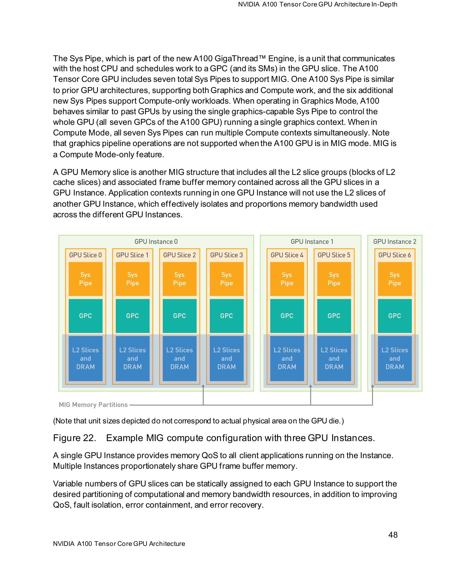
解读: MIG分区示例展示单颗A100被分为多个GPU Instance,每个实例拥有独立SM集合、L2 Cache slice和显存分区。图中可见不同大小的实例混合配置(如3g.20gb + 2g.10gb + 1g.5gb等)。关键: 每个实例有独立的memory controller通路,确保带宽QoS——一个实例的HBM流量不会干扰另一个实例。MIG的7-instance上限由memory controller数量(10个)和SM分组粒度(~14 SM/slice)决定。
6c. Scale-Out Interface #
7. Power, Thermal & Efficiency #
| Parameter | Value |
|---|---|
| TDP (SXM4) | 400W |
| TDP (PCIe) | 250W |
| Cooling | Air (SXM4 baseboard), Passive heatsink (PCIe) |
| Process Power Efficiency | TSMC 7nm N7 |
7a. 能效代际对比 #
| Metric | V100 SXM2 (300W) | A100 SXM4 (400W) | Improvement |
|---|---|---|---|
| FP16 TC TFLOPS/W | \( 125/300 = 0.417 \) | \( 312/400 = 0.780 \) | 1.87x |
| FP16 Sparse TFLOPS/W | — | \( 624/400 = 1.560 \) | — |
| TF32 TC TFLOPS/W | — | \( 156/400 = 0.390 \) | — |
| FP64 TC TFLOPS/W | — | \( 19.5/400 = 0.049 \) | — |
| FP32 CUDA TFLOPS/W | \( 15.7/300 = 0.052 \) | \( 19.5/400 = 0.049 \) | 0.93x |
| INT8 TC TOPS/W | \( 62/300 = 0.207 \) | \( 624/400 = 1.560 \) | 7.5x |
A100能效提升核心来自TC重设计(2x/SM)和工艺12nm→7nm,而非单纯堆料(SM数仅+35%)。TC workload能效1.87x远优于FP32 CUDA(略降)——NVIDIA将晶体管预算优先分配给TC吞吐和cache而非CUDA core。
8. Software & ISA Impact #
8a. ISA Changes (Compute Capability 8.0) #
新增指令:
8b. 编译器与软件栈 #
8c. 编程模型变化 #
9. AI Workload Impact Analysis #
9a. GEMM (矩阵乘法) #
9b. Attention #
9c. MoE (Mixture of Experts) #
9d. Training vs Inference #
10. Competitive Positioning — A100 vs AMD MI100 / MI250X #
| Metric | A100 SXM4 (80GB) | AMD MI100 (2020) | AMD MI250X (2021) |
|---|---|---|---|
| Process | TSMC 7nm | TSMC 7nm | TSMC N6 |
| Die Size | 826 mm² (mono) | 750 mm² (mono) | 2× 228 mm² (MCM) |
| Transistors | 54.2B | 26.8B | 58B (2 GCDs) |
| CUs/SMs | 108 SMs | 120 CUs | 220 CUs (110×2) |
| FP16 Matrix | 312 TFLOPS | 184.6 TFLOPS | 383 TFLOPS |
| FP64 Matrix | 19.5 TFLOPS | 46.1 TFLOPS | 95.7 TFLOPS |
| FP32 Vector | 19.5 TFLOPS | 23.1 TFLOPS | 47.9 TFLOPS |
| Memory | 80 GB HBM2e | 32 GB HBM2 | 128 GB HBM2e |
| Bandwidth | 2,039 GB/s | 1,228 GB/s | 3,276 GB/s |
| Interconnect | NVLink 600 GB/s | IF 276 GB/s | IF 800 GB/s (inter-GCD) |
| TDP | 400W | 300W | 500W |
| Sparsity | 2:4 Structured | No | No |
| MIG | Yes (7 inst.) | No | No |
| Software | CUDA (dominant) | ROCm (early) | ROCm (maturing) |
竞品分析:
11. Comprehensive Spec Sheet #
| Category | Parameter | A100 SXM4 (80GB) |
|---|---|---|
| Architecture | Architecture Name | NVIDIA Ampere |
| GPU Code Name | GA100 | |
| Process Node | TSMC 7nm N7 | |
| Die Size | 826 mm² | |
| Transistors | 54.2 billion | |
| Packaging | Monolithic die | |
| Compute | GPCs | 7 (+1 partial) |
| TPCs | ~54 | |
| SMs | 108 | |
| CUDA Cores (FP32) | 6,912 (64/SM) | |
| INT32 Cores | 6,912 (64/SM) | |
| FP64 Units | 3,456 (32/SM) | |
| Tensor Cores | 432 (4/SM, 3rd gen) | |
| Boost Clock | 1,410 MHz | |
| TC Performance | FP64 TC | 19.5 TFLOPS |
| TF32 TC | 156 TFLOPS (312 sparse) | |
| BF16 TC | 312 TFLOPS (624 sparse) | |
| FP16 TC | 312 TFLOPS (624 sparse) | |
| INT8 TC | 624 TOPS (1,248 sparse) | |
| INT4 TC | 1,248 TOPS (2,496 sparse) | |
| CUDA Performance | FP64 | 9.7 TFLOPS |
| FP32 | 19.5 TFLOPS | |
| FP16 | 78 TFLOPS | |
| BF16 | 39 TFLOPS | |
| Memory | HBM Type | HBM2e |
| Capacity | 80 GB | |
| Stacks | 5 | |
| Controllers | 10 × 512-bit | |
| Bandwidth | 2,039 GB/s | |
| L2 Cache | 40 MB | |
| L1/SMEM per SM | 192 KB | |
| Register File per SM | 256 KB | |
| Interconnect | NVLink Version | 3.0 |
| NVLink Links | 12 | |
| NVLink BW (bidir) | 600 GB/s | |
| PCIe | Gen 4 x16 (64 GB/s) | |
| Power | TDP (SXM4) | 400W |
| TDP (PCIe) | 250W | |
| FP16 TC TFLOPS/W | 0.780 | |
| Features | MIG | Up to 7 GPU Instances |
| Sparsity | 2:4 Structured | |
| Async Copy | Global → Shared Memory | |
| Compute Capability | 8.0 |
12. Infrastructure Impact #
| Layer | Impact |
|---|---|
| Algorithm | TF32使FP32训练自动获得TC加速,降低混合精度算法调整需求;2:4 Sparsity催生结构化剪枝算法(ASP, SR-STE);FP64 TC加速迭代精化求解器(TCAIRS)改变HPC算法设计 |
| Kernel | Async Copy引入multi-stage pipeline优化范式(3-4 stage prefetch+compute overlap);192KB SMEM允许更大tile(128×128+) → TC utilization提升;L2 Residency Control需要kernel-level cache management策略 |
| Framework | cuBLAS默认启用TF32(零代码修改);AMP(torch.cuda.amp)无缝利用FP16/BF16 TC;cuSPARSELt新API用于稀疏GEMM;MIG需要框架支持GPU分区感知调度 |
| LLM | 80GB可容纳GPT-2级别(1.5B FP16=3GB)但不够GPT-3(175B FP16=350GB需5卡);TF32默认加速使LLM训练从V100迁移零改动;大L2缓解embedding table random access |
| Agent | MIG允许同一GPU运行多推理实例 → 多agent共享GPU;INT8 TC(624 TOPS)提供高吞吐推理 |
| Cluster | DGX A100(8×A100 + NVSwitch)成为AI训练"标准单元"(5 PFLOPS);NVLink 600GB/s + HDR IB 200Gbps定义TP/DP带宽边界;MIG使CSP可切分单GPU为多个计费实例 |