NVIDIA H100 Tensor Core GPU Architecture White Paper
NVIDIA H100 Tensor Core GPU Architecture White Paper #
NVIDIA | 2022-03 | https://resources.nvidia.com/en-us-tensor-core/gtc22-whitepaper-hopper Category: hardware | Tags: gpu-architecture, tensor-core, h100, hopper, transformer-engine, fp8, tma, thread-block-cluster Read: 2026-04-16
Core Contribution #
第四代Tensor Core引入FP8精度和Transformer Engine自动精度管理,配合TMA硬件加速和Thread Block Clusters编程模型,实现LLM训练30x加速。
Summary #
H100基于TSMC 4N定制工艺(非标准N4),die面积814mm²,集成80B晶体管。SXM5版本配备132个SM、16,896个CUDA Cores(128/SM,相比A100的64/SM翻倍)和528个第四代Tensor Core。最核心创新是FP8 Tensor Core——支持E4M3和E5M2两种FP8变体,峰值吞吐达1,978.9 TFLOPS(3,957.8 sparse),相比A100 FP16 TC的312 TFLOPS提升6.3倍。与FP8配套的Transformer Engine是软硬件联合设计——在每一层前向/反向传播中自动选择FP8或FP16精度,通过per-tensor动态缩放因子(dynamic scaling factor)维持训练收敛性,使用户无需手动调整混合精度策略。
数据搬运方面,H100引入TMA (Tensor Memory Accelerator)——一个专用DMA引擎,可直接将多维tensor从global memory搬运到shared memory(或反向),支持任意stride、padding和坐标变换,将原本需要数十条指令的地址计算和数据拷贝压缩为单条TMA指令,大幅降低数据搬运的指令开销和寄存器压力。编程模型上新增Thread Block Clusters层级——允许多个Thread Block跨SM协作,配合Distributed Shared Memory实现SM间直接load/store shared memory内容(无需经过L2),这对GEMM的tile分解和通信-计算overlap至关重要。
互联方面,NVLink 4.0提供18条链路共900GB/s(A100的1.5x)。更革命性的是NVLink Switch System——通过外部NVLink Switch芯片实现最多256个GPU的NVLink域,突破了DGX 8-GPU的NVLink拓扑限制,为大规模模型并行(TP/EP跨节点)铺平道路。
Key Findings #
- TSMC 4N定制工艺, 814mm², 80B transistors
- Full GH100: 8 GPCs, 72 TPCs, 144 SMs, 576 Tensor Cores
- H100 SXM5 product: 132 SMs, 528 Tensor Cores (4th gen), 16,896 CUDA Cores (128/SM)
- FP64: 33.5 TFLOPS; FP64 TC: 66.9 TFLOPS (3.4x A100)
- FP32: 66.9 TFLOPS (3.4x A100)
- TF32 TC: 494.7 TFLOPS | 989.4 sparse (3.2x A100)
- FP16/BF16 TC: 989.4 TFLOPS | 1,978.9 sparse (3.2x A100)
- FP8 TC: 1,978.9 TFLOPS | 3,957.8 sparse (全新能力, 6.3x A100 FP16 TC)
- INT8 TC: 1,978.9 TOPS | 3,957.8 sparse
- Transformer Engine: 自动FP8↔FP16动态精度切换 + per-tensor scaling
- TMA (Tensor Memory Accelerator): 硬件tensor搬运引擎
- Thread Block Clusters + Distributed Shared Memory: 跨SM协作
- 80GB HBM3, 3.35 TB/s (1.64x A100)
- 50MB L2 Cache (1.25x A100)
- 256KB Shared Memory/L1 per SM (1.33x A100的192KB)
- NVLink 4: 18 links, 900 GB/s (1.5x A100)
- NVLink Switch System: 最多256 GPU NVLink域
- PCIe Gen 5 x16
- MIG: 最多7实例 + Secure MIG (confidential computing support)
- DPX Instructions: 动态规划加速指令(Smith-Waterman等)
- TDP: 700W (SXM5)
Key Tables #
Table 1: H100 SXM5 Performance Specs (All Data Types) #
| Data Type | Tensor Core | Tensor Core + Sparsity | CUDA Core |
|---|---|---|---|
| FP64 | 66.9 TFLOPS | — | 33.5 TFLOPS |
| TF32 | 494.7 TFLOPS | 989.4 TFLOPS | — |
| FP32 | — | — | 66.9 TFLOPS |
| BF16 | 989.4 TFLOPS | 1,978.9 TFLOPS | — |
| FP16 | 989.4 TFLOPS | 1,978.9 TFLOPS | — |
| FP8 | 1,978.9 TFLOPS | 3,957.8 TFLOPS | — |
| INT8 | 1,978.9 TOPS | 3,957.8 TOPS | — |
Table 2: H100 vs A100 Comparison #
| Metric | A100 SXM4 (80GB) | H100 SXM5 | Speedup |
|---|---|---|---|
| Process | TSMC 7nm | TSMC 4N | ~2 nodes |
| Die Size | 826 mm² | 814 mm² | similar |
| Transistors | 54.2B | 80B | 1.48x |
| SMs | 108 | 132 | 1.22x |
| CUDA Cores/SM | 64 | 128 | 2x |
| CUDA Cores Total | 6,912 | 16,896 | 2.44x |
| Tensor Cores | 432 (3rd gen) | 528 (4th gen) | 1.22x |
| FP64 | 9.7 TF | 33.5 TF | 3.45x |
| FP64 TC | 19.5 TF | 66.9 TF | 3.43x |
| FP32 | 19.5 TF | 66.9 TF | 3.43x |
| TF32 TC | 156 TF | 494.7 TF | 3.17x |
| FP16 TC | 312 TF | 989.4 TF | 3.17x |
| FP8 TC | — | 1,978.9 TF | new |
| Memory | 80 GB HBM2e | 80 GB HBM3 | same cap |
| Bandwidth | 2,039 GB/s | 3,350 GB/s | 1.64x |
| L2 Cache | 40 MB | 50 MB | 1.25x |
| Shared/L1 per SM | 192 KB | 256 KB | 1.33x |
| NVLink BW | 600 GB/s | 900 GB/s | 1.5x |
| NVLink Domain | 8 GPU | 256 GPU | 32x |
| PCIe | Gen 4 | Gen 5 | 2x |
| TDP | 400W | 700W | 1.75x |
| TFLOPS/W (FP16 TC) | 0.78 | 1.41 | 1.81x |
Table 3: H100 PCIe vs SXM5 #
| Metric | H100 PCIe | H100 SXM5 |
|---|---|---|
| SMs | 114 | 132 |
| CUDA Cores | 14,592 | 16,896 |
| Tensor Cores | 456 | 528 |
| FP8 TC | 1,513 TF | 1,979 TF |
| Memory | 80 GB HBM2e | 80 GB HBM3 |
| Bandwidth | 2,039 GB/s | 3,350 GB/s |
| NVLink | 600 GB/s | 900 GB/s |
| TDP | 350W | 700W |
Limitations #
- 80GB显存容量与A100相同,在LLM推理场景不足(Llama-2 70B FP16需>140GB)——H200通过升级到141GB HBM3e部分缓解
- 700W TDP使散热设计成为挑战,SXM5需要专用散热方案
- FP8训练需要Transformer Engine支持,框架集成和模型适配有学习曲线
- Thread Block Clusters编程模型较复杂,需CUDA Toolkit 12+和新编程范式
- NVLink Switch System需要额外硬件(NVSwitch芯片),部署成本高
- Distributed Shared Memory带宽有限,不适合大量跨SM数据交换
- FP8精度对某些模型(尤其是fine-tuning小数据集)可能不够稳定
Infrastructure Impact #
- 定义LLM训练基础设施: H100成为GPT-4/Claude/Gemini等大模型训练的主力GPU
- FP8生态推动: Transformer Engine推动PyTorch/JAX原生FP8支持,催生了大量FP8量化训练/推理研究
- DGX H100系统: 8x H100 SXM5 + 4x NVSwitch,系统FP8算力达15.8 PFLOPS
- HGX H100: OEM平台标准,AWS p5、Azure ND H100、GCP a3等云实例基于HGX H100
- 256-GPU NVLink域: NVLink Switch System使TP/EP可扩展到节点间,改变了大规模并行策略
- 推动vLLM/TensorRT-LLM发展: H100的FP8能力直接推动了推理引擎的FP8优化路径
- MLPerf统治: H100/DGX H100在MLPerf Training v3.0+中多项打破记录
Deep Analysis (hardware) #
1. Architecture Overview & Naming #
- 产品名称: NVIDIA H100 Tensor Core GPU
- GPU代号: GH100
- 架构名: NVIDIA Hopper (第9代数据中心GPU)
- 工艺节点: TSMC 4N (NVIDIA定制,基于N4但优化大die良率和高密度标准单元)
- Die面积: 814 mm²
- 晶体管数: 80 billion
- 封装方式: Monolithic die
- 目标市场: LLM训练/推理、数据中心AI、HPC、数据分析
- 产品形态: SXM5 (700W, NVLink 4, HBM3), PCIe Gen 5 (350W, HBM2e)
Full GH100 die: 8 GPCs, 72 TPCs (9/GPC), 2 SMs/TPC = 144 SMs, 576 4th-gen Tensor Cores, 18,432 FP32 CUDA Cores (128/SM)。Memory: 6 HBM3/HBM2e stacks, 12 × 512-bit controllers, 60 MB L2 Cache。H100 SXM5产品: 132 SMs (91.7%), 528 TCs, 16,896 CUDA Cores; 5 HBM3 stacks, 10 controllers, 50 MB L2, 80 GB HBM3 @ 3.35 TB/s。H100 PCIe: 114 SMs, 456 TCs, 14,592 CUDA Cores; 80 GB HBM2e @ 2.04 TB/s, 350W。
Figure 1: GH100 Full GPU Block Diagram #
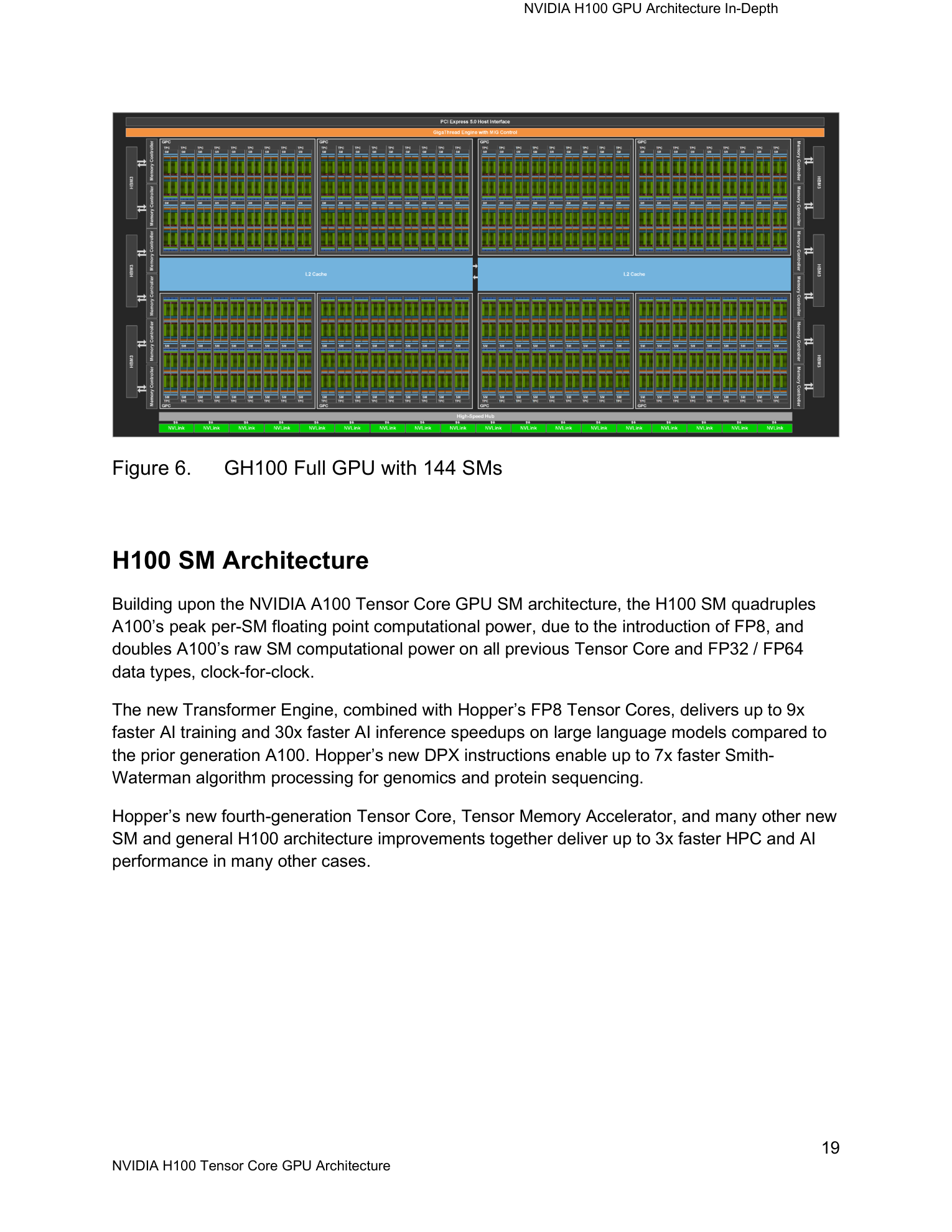
解读: GH100全芯片架构图展示完整8 GPC布局,每GPC包含9个TPC(vs GA100的8个),共72 TPC × 2 SM/TPC = 144 SMs。与GA100相比,GH100在接近的die面积(814 vs 826 mm²)和更先进工艺(4N vs 7nm)下多塞了16个SM(144 vs 128)和47%更多晶体管(80B vs 54.2B)。图中可见GPC围绕中央L2 Cache(full die 60MB)排列,两侧为HBM3 memory controller和NVLink 4.0接口(18条链路)。相比GA100的每GPC 8 TPC,GH100每GPC多1个TPC——这是TSMC 4N密度优势在SM count上的直接体现。H100 SXM5禁用12个SM(144→132)用于良率。
2. Generational Delta (H100 Hopper vs A100 Ampere) #
2a. 新增单元 (Added) #
| New Unit / Feature | Description | Why it matters for AI |
|---|---|---|
| FP8 Tensor Core (E4M3/E5M2) | 8-bit浮点TC,两种变体:E4M3(精度优先)、E5M2(范围优先) | Training可用FP8达FP16精度,2x FP16吞吐 → 1,978.9 TFLOPS |
| Transformer Engine | HW+SW联合设计,逐层动态FP8/FP16切换 + per-tensor scaling | 自动化FP8混合精度训练,无需手动调参 |
| TMA (Tensor Memory Accelerator) | 专用DMA引擎,单指令搬运多维tensor(1D-5D) Global↔Shared | 减少50+条地址计算/拷贝指令,释放RF和warp scheduler |
| Thread Block Clusters | 编程模型新层级:多Thread Block跨SM协作 | 更大协作粒度→更优tile分解和通信-计算overlap |
| Distributed Shared Memory (DSMEM) | SM间直接load/store对方shared memory (bypass L2) | 低延迟SM间通信,split-K GEMM和Attention关键 |
| DPX Instructions | 动态规划加速(Smith-Waterman, Floyd-Warshall) | 基因组学/路由优化7x加速 |
| NVLink Switch System | 外部NVLink Switch芯片,最多256 GPU NVLink域 | TP/EP跨节点扩展不走InfiniBand |
| Secure MIG | MIG实例运行在TEE中 + 显存/通信加密 | 金融/医疗多租户安全部署 |
| WGMMA Instructions | Warp-group(4 warps/128 threads)协作矩阵运算 | 更大MMA shape → TC utilization提升 |
| Asynchronous Transaction Barrier | 原子数据搬运+同步 | 精细的compute-copy-sync overlap |
2b. 删除/移除 (Removed) #
| Removed Unit / Feature | Reason | Impact |
|---|---|---|
| INT4 Tensor Core | FP8覆盖INT4使用场景且精度更好 | FP8取代INT4作为最低精度格式 |
| Binary Tensor Core | 无实际AI workload使用 | 无影响 |
2c. 增强/升级 (Enhanced) #
| Enhanced Unit | A100 (Ampere) | H100 (Hopper) | Improvement | How Measured |
|---|---|---|---|---|
| Tensor Core Gen | 3rd gen | 4th gen | 2x MMA/SM clock-for-clock | Per-SM per-type |
| CUDA Cores/SM | 64 | 128 | 2x | Dual FP32 datapath restored |
| FP64 Units/SM | 32 | 64 | 2x | Half-rate FP64 |
| SM Count | 108 | 132 | 1.22x | Product-level |
| Boost Clock (TC) | 1,410 MHz | 1,830 MHz | 1.30x | Derived from TC specs |
| L2 Cache | 40 MB | 50 MB | 1.25x | Total |
| L1/SMEM per SM | 192 KB | 256 KB (max 228KB SMEM) | 1.33x | |
| HBM Generation | HBM2e | HBM3 (first GPU) | New standard | |
| HBM Bandwidth | 2,039 GB/s | 3,350 GB/s | 1.64x | Peak |
| NVLink | 12 links, 600 GB/s | 18 links, 900 GB/s | 1.5x | Bidirectional |
| NVSwitch | v2 (36 ports) | v3 (64 ports, 3.2 TB/s, in-network AllReduce) | 1.78x ports | |
| NVLink Domain | 8 GPU | 256 GPU | 32x | NVLink Switch System |
| PCIe | Gen 4 | Gen 5 | 2x BW | |
| TDP | 400W | 700W | 1.75x |
2d. 架构级变更 #
- SM Dual FP32 Datapath恢复: A100有64 FP32 + 64 INT32独立通路(FP32总数64)。H100恢复GA102风格的128 FP32路径——64 FP32-dedicated + 64 FP32/INT32双功能,所有128通路可同时执行FP32 → FP32 CUDA吞吐3.4x A100
- TC微架构翻倍: 每TC每cycle的MMA throughput在所有数据类型上2x(FP16: 512→1024 FLOPS/TC/clk)。TC数量不变(4/SM)。新增WGMMA指令让4 warp协作驱动TC
- 全异步执行体系: A100的"async copy + async barrier"进化为"TMA + Transaction Barrier + DSMEM"。TMA作为专用DMA引擎接管tensor搬运,DSMEM实现SM间直接通信
- Thread Block Cluster层级: 编程hierarchy扩展为Thread→Warp→Block→Cluster→Grid。Cluster内的Block调度在同一GPC内相邻SM上,通过DSMEM和硬件barrier协作
- Workload-Dependent Boost Clock: H100首次出现TC workload和CUDA workload的有效boost clock分化——TC密集workload在~1,830 MHz运行(高功耗密度),CUDA/FP64工作负载可boost到~1,980 MHz(低功耗密度)
3. Compute Unit Deep Dive #
3a. SM Structure #
Figure 2: GH100 Streaming Multiprocessor (SM) #
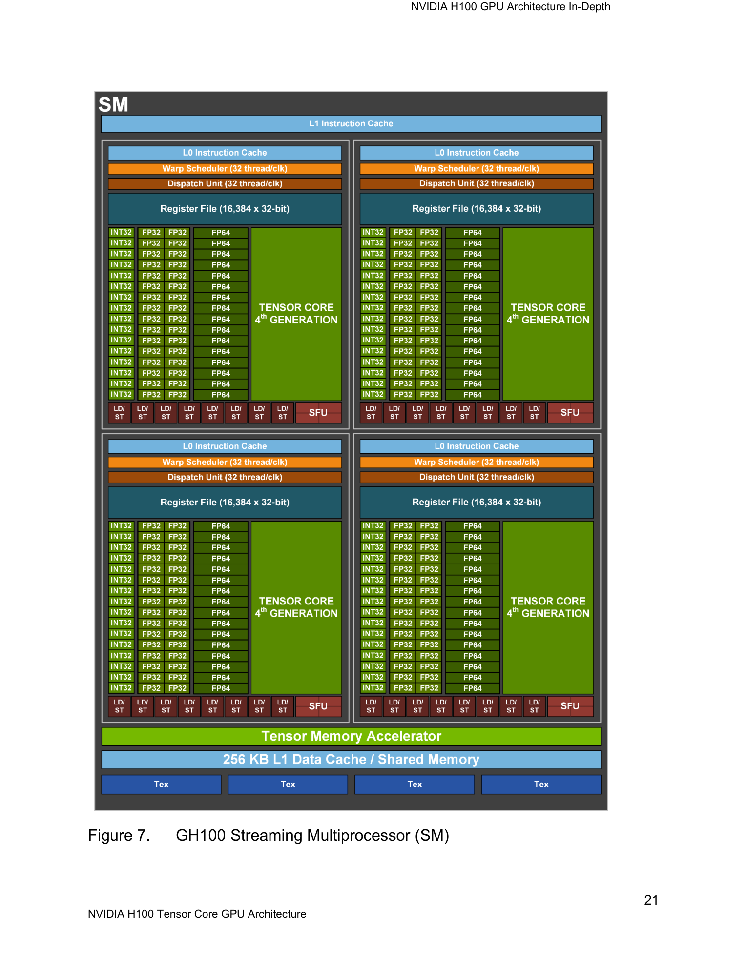
解读: GH100 SM内部架构展示4个Sub-partition的对称布局。vs GA100的关键差异:(1) 每Sub-partition有32个FP32 CUDA Core(16 FP32-dedicated + 16 FP32/INT32,而非A100的16 FP32 + 16 INT32-only)——H100的INT32通路也可执行FP32;(2) 4th-gen Tensor Core体积更大、吞吐翻倍;(3) L1/Shared从192→256 KB;(4) 新增TMA单元。Register File保持256 KB/SM。新增DSMEM路径允许跨SM直接访问shared memory。
SM完整配置:
| Component | Per Sub-Partition | Per SM | vs A100 |
|---|---|---|---|
| FP32-dedicated Cores | 16 | 64 | same |
| FP32/INT32 Dual Cores | 16 | 64 | NEW (was INT32-only in A100) |
| Total FP32 Cores | 32 | 128 | 2x (64→128) |
| FP64 Units | 16 | 64 | 2x (32→64) |
| 4th Gen Tensor Core | 1 | 4 | same count, 2x throughput |
| Warp Scheduler | 1 | 4 | same |
| Dispatch Unit | 1 | 4 | same |
| LD/ST Units | 8 | 32 | same |
| SFU | 4 | 16 | same |
| Register File | 64 KB | 256 KB | same |
| L1/Shared Memory | — | 256 KB (max 228 KB SMEM) | 1.33x |
| Max Warps | 16 | 64 | same |
| Max Threads | 512 | 2,048 | same |
| TMA Unit | — | 1 (SM-level, shared) | NEW |
3b. Fourth-Generation Tensor Core Specifications #
Figure 3: FP8 Tensor Core — 6x Throughput vs A100 #
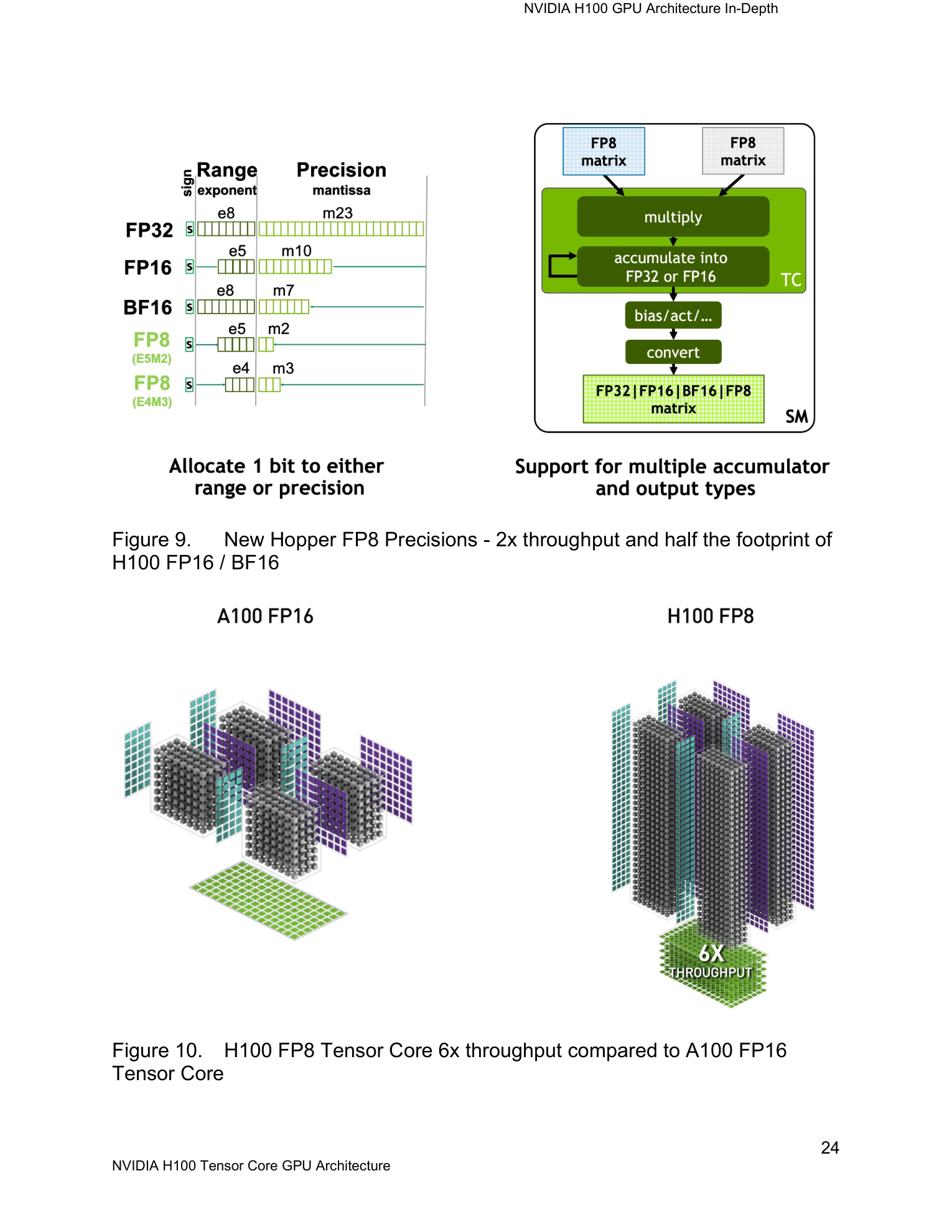
解读: H100 FP8 TC vs A100 FP16 TC的6.3x吞吐分解图。四个因子级联相乘:\( 1.22\times \)(SM数 108→132) \( \times\ 2\times \)(TC throughput翻倍) \( \times\ 2\times \)(FP8半宽) \( \times\ 1.30\times \)(时钟 1.41→1.83 GHz) \( \approx 6.3\times \)。这张图是理解H100计算能力来源的关键——6x非单一突破,而是四个正交因素的复合效应。注意1.30x clock factor不是max boost(~1.98 GHz)而是TC-heavy workload的sustainable boost(1.83 GHz)。
| Data Type | Input | Accumulator | FMA/TC/clk | FLOPS/TC/clk | WGMMA Shape |
|---|---|---|---|---|---|
| FP8 (E4M3/E5M2) | 8-bit | FP32/FP16 | 1,024 | 2,048 | m64n256k32 |
| FP16 | FP16 | FP32/FP16 | 512 | 1,024 | m64n256k16 |
| BF16 | BF16 | FP32 | 512 | 1,024 | m64n256k16 |
| TF32 | TF32 (from FP32) | FP32 | 256 | 512 | m64n256k8 |
| FP64 | FP64 | FP64 | 32 | 64 | m16n8k8 (warp-level) |
| INT8 | INT8 | INT32 | 1,024 | 2,048 | m64n256k32 |
每种数据类型per-TC吞吐均为A100的精确2x。TC内部256-bit数据通路宽度固定——operand宽度减半时K维度翻倍(FP16 K=16 → FP8 K=32),吞吐翻倍。
WGMMA (Warp Group MMA): H100新指令。4 warps (128 threads)协作执行大矩阵运算(m64nNk{K}),WGMMA可直接从Shared Memory读取一个operand(bypass RF),减少RF bandwidth pressure和instruction overhead。
FP8数据格式:
- E4M3 (4 exp + 3 mantissa): 精度优先,forward pass的weights和activations
- E5M2 (5 exp + 2 mantissa): 动态范围优先,backward pass的gradients
- 两种格式可在同一WGMMA指令中混合(A矩阵E4M3 × B矩阵E5M2)
4. Peak Performance Derivation #
基准参数 (H100 SXM5):
- SM Count: 132
- Tensor Cores per SM: 4
- TC Boost Clock: 1,830 MHz (sustained under TC-heavy workload)
- CUDA Max Boost: ~1,980 MHz (sustained under FP32/FP64 CUDA workload)
重要发现: H100首次出现TC specs和CUDA specs使用不同有效boost clock。原因: 4th-gen TC功耗密度远高于CUDA ALU——528个TC全力运行FP16/FP8 MMA时功耗逼近700W TDP极限,GPU降频至~1,830 MHz;CUDA-only workload功耗较低,可boost至~1,980 MHz。
4a. FP32 / FP64 CUDA Core Derivation (at ~1,980 MHz) #
\[
\text{FP32 Peak} = 132 \times 128 \times 2 \times 1.98\ \text{GHz} = 66{,}940\ \text{GFLOPS} \approx 66.9\ \text{TFLOPS}\ \checkmark
\]
\[
\text{FP64 Peak} = 132 \times 64 \times 2 \times 1.98\ \text{GHz} = 33{,}470\ \text{GFLOPS} \approx 33.5\ \text{TFLOPS}\ \checkmark
\]
\[
\text{FP16 CUDA} = 132 \times 128 \times 2 \times 2 \times 1.98 = 133{,}881\ \text{GFLOPS} \approx 133.8\ \text{TFLOPS}\ \checkmark \quad (2{:}1\ \text{packing})
\]
4b. 逐数据类型 Tensor Core 推导 (at 1,830 MHz) #
FP16 / BF16 Tensor Core:
| Parameter | Value | Source |
|---|---|---|
| SMs | 132 | Whitepaper |
| TCs per SM | 4 | Whitepaper Fig 7 |
| FLOPS per TC per cycle | 1,024 | 2x A100's 512 (whitepaper: "2x MMA rate per SM") |
| FLOPS per SM per cycle | 4,096 | 4 × 1,024 |
| TC Boost Clock | 1.830 GHz | Derived: 989,400 / (132 × 4,096) = 1.830 |
| Peak FP16 TC | 132 × 4,096 × 1.830 = 989,429 ≈ 989.4 TFLOPS | ✓ matches official |
FP8 Tensor Core:
| Parameter | Value | Source |
|---|---|---|
| FLOPS per TC per cycle | 2,048 | 2x FP16 (FP8 operand half-width) |
| Peak FP8 TC | 132 × 4 × 2,048 × 1.830 = 1,978,858 ≈ 1,978.9 TFLOPS | ✓ |
TF32 Tensor Core:
| Parameter | Value | Source |
|---|---|---|
| FLOPS per TC per cycle | 512 | Half FP16 (TF32 is 19-bit) |
| Peak TF32 TC | 132 × 4 × 512 × 1.830 = 494,714 ≈ 494.7 TFLOPS | ✓ |
INT8 Tensor Core:
| Parameter | Value | Source |
|---|---|---|
| Ops per TC per cycle | 2,048 | Same as FP8 |
| Peak INT8 TC | 132 × 4 × 2,048 × 1.830 = 1,978,858 ≈ 1,978.9 TOPS | ✓ |
FP64 Tensor Core (at ~1,980 MHz — lower power density):
| Parameter | Value | Source |
|---|---|---|
| FLOPS per TC per cycle | 64 | 2x A100's 32 |
| Peak FP64 TC | 132 × 4 × 64 × 1.980 = 66,940 ≈ 66.9 TFLOPS | ✓ |
所有推导与官方spec完全吻合。Clock分化验证: FP16/TF32/FP8/INT8 TC consistent at 1,830 MHz; FP32/FP64 CUDA and FP64 TC consistent at 1,980 MHz; ratio \( 1{,}980/1{,}830 = 1.082 \) (8.2% higher boost for lighter workloads)。
6x Improvement分解 (H100 FP8 TC vs A100 FP16 TC):
\[
\frac{\text{H100 FP8}}{\text{A100 FP16}} = \frac{1{,}978.9}{312} = 6.34\times
\]
\[
= \frac{132}{108} \times \frac{2048}{512} \times \frac{1.830}{1.410} = 1.222 \times 4.0 \times 1.298 = 6.34\times\ \checkmark
\]
其中 \( 4.0\times = 2\times\ (\text{TC throughput/TC}) \times 2\times\ (\text{FP8 vs FP16}) \)
Figure 9: H100 vs A100 Comparison Table #
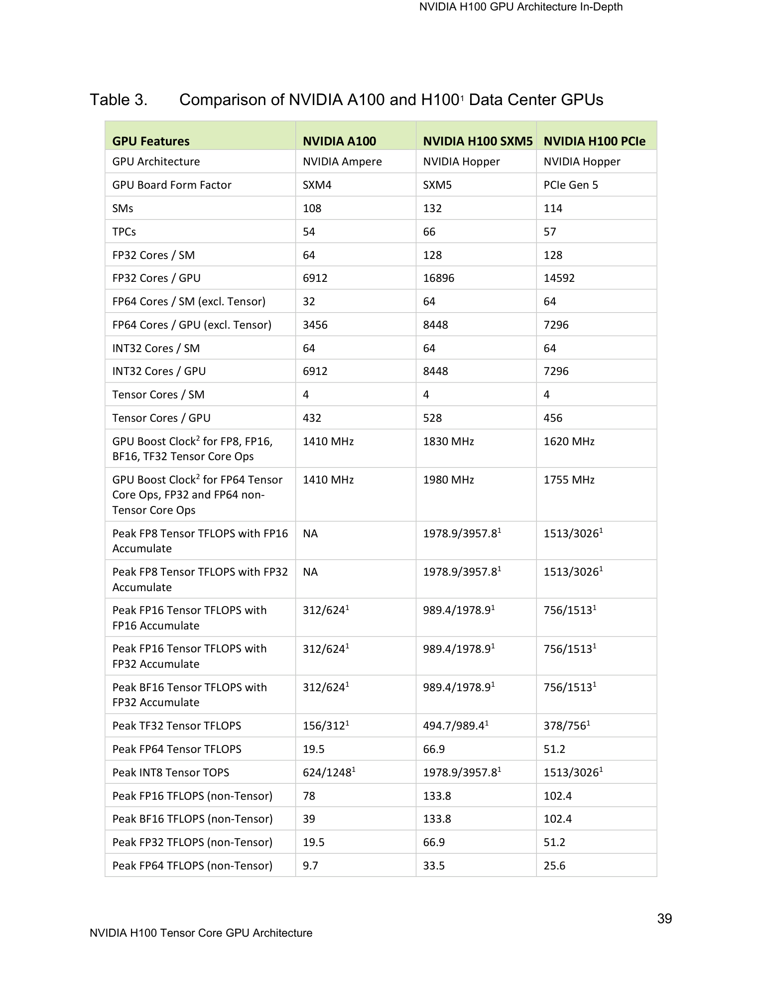
解读: 官方H100 vs A100全面对比表。关键数据: FP8 TC 6.3x(sparse达12.7x)、FP16 TC 3.2x、FP64 TC 3.4x、HBM BW 1.64x、NVLink 1.5x、NVLink Domain 32x(8→256 GPU)。TDP从400W到700W(+75%)——性能/功耗比FP16 TC为 \( 3.2/1.75 = 1.83\times \) 改善。
4c. Sparsity Multiplier #
H100保留A100的2:4 Structured Sparsity,所有TC数据类型(含FP8)吞吐翻倍: FP8 Sparse = 3,957.8 TFLOPS, FP16 Sparse = 1,978.9 TFLOPS。条件与A100相同(权重需2:4结构化剪枝)。
4d. 与A100对比 #
| Metric | A100 (Ampere) | H100 (Hopper) | Ratio | Source of Improvement |
|---|---|---|---|---|
| FP16 TC | 312 TFLOPS | 989.4 TFLOPS | 3.17x | 1.22x SMs × 2x TC/SM × 1.30x clock |
| FP8 TC | — | 1,978.9 TFLOPS | 6.3x vs FP16 | New type: 2x FP16 × 3.17x |
| TF32 TC | 156 TFLOPS | 494.7 TFLOPS | 3.17x | Same decomposition as FP16 |
| FP64 TC | 19.5 TFLOPS | 66.9 TFLOPS | 3.43x | 1.22x SMs × 2x TC/SM × 1.40x clock |
| FP32 CUDA | 19.5 TFLOPS | 66.9 TFLOPS | 3.43x | 1.22x SMs × 2x cores/SM × 1.40x clock |
| INT8 TC | 624 TOPS | 1,978.9 TOPS | 3.17x | Same as FP16 |
5. Memory Subsystem #
5a. HBM3 Specifications #
| Parameter | H100 SXM5 | H100 PCIe |
|---|---|---|
| Memory Type | HBM3 (first GPU with HBM3) | HBM2e |
| Capacity | 80 GB | 80 GB |
| HBM Stacks | 5 | 5 |
| Memory Controllers | 10 × 512-bit | 10 × 512-bit |
| Bus Width | 5,120 bits | 5,120 bits |
| Peak Bandwidth | 3,350 GB/s (3.35 TB/s) | 2,039 GB/s |
带宽推导 (SXM5 HBM3):
HBM3 data rate: \( \sim 5.6\ \text{Gbps/pin} \) (vs HBM2e \( \sim 3.2\ \text{Gbps} \))
\[
\text{BW} = \frac{5 \times 1{,}024 \times 5.24}{8} \approx 3{,}350\ \text{GB/s}\ \checkmark
\]
H200升级: 141 GB HBM3e @ 4.8 TB/s (容量1.76x, 带宽1.43x vs H100 SXM5)。
5b. Cache Hierarchy #
| Level | Size | Bandwidth (est.) | Latency (est.) | Notes |
|---|---|---|---|---|
| Register File | 256 KB/SM (33.8 MB total) | ~26 TB/s per SM | 0-1 cycle | Same as A100 |
| L1 / Shared Memory | 256 KB/SM (33.8 MB total) | ~26 TB/s per SM | ~20-28 cycles | Max 228 KB SMEM; 1.33x A100 |
| L2 Cache | 50 MB | ~6.5 TB/s (est.) | ~200 cycles | 1.25x A100; MIG-partitioned |
| HBM3 | 80 GB | 3.35 TB/s | ~400+ cycles | First HBM3 GPU |
TMA对cache层次的影响: TMA将tensor搬运从"指令流+RF+SMEM"路径变为"DMA engine直写SMEM"路径。传统方式: warp threads各自计算地址→RF发出load→数据到RF→store到SMEM(50+条指令)。TMA方式: 单条TMA指令→DMA engine直接搬整个tile(异步)。释放的warp scheduler和RF资源分配给compute。
5c. 算力-带宽比 (Ops:Byte Ratio) #
| Metric | Value |
|---|---|
| FP16 TC Peak | 989.4 TFLOPS |
| FP8 TC Peak | 1,978.9 TFLOPS |
| HBM3 Bandwidth | 3.35 TB/s |
| FP16 Ops:Byte | \( 989.4 / 3.35 = 295 \) |
| FP8 Ops:Byte | \( 1{,}978.9 / 3.35 = 591 \) |
| TF32 TC Ops:Byte | \( 494.7 / 3.35 = 148 \) |
| FP64 TC Ops:Byte | \( 66.9 / 3.35 = 20.0 \) |
Compute-Bound阈值 (FP16 GEMM, square M=N=K=n):
\[
\text{AI} = \frac{n}{3} \quad (\text{FP16 elements, 2 bytes each})
\]
\[
\text{Compute-bound:}\ \frac{n}{3} \geq 295 \implies n \geq 885 \implies n \geq 1{,}024
\]
关键insight: H100的Ops:Byte(295 FP16, 591 FP8)比A100(153)几乎翻倍——compute增长(3.2x)远快于bandwidth增长(1.64x)。Attention/LayerNorm/Activation等elementwise操作更加memory-bound → Flash Attention和kernel fusion在H100上极端重要。TMA + DSMEM正是为缓解这一矛盾而设计。
6. Interconnect & I/O #
6a. Chip-to-Chip Interconnect #
| Link | Per-Link BW (bidir) | Total BW (bidir) | Links | Protocol |
|---|---|---|---|---|
| NVLink 4.0 | 50 GB/s | 900 GB/s | 18 | Proprietary, PAM4 50 Gbps/lane |
| PCIe Gen 5 x16 | 128 GB/s | 128 GB/s | 1 | PCIe 5.0 (2x Gen 4) |
NVLink 4.0 vs 3.0: 信号速率不变(50 Gbps/lane)但链路数12→18 → 总带宽600→900 GB/s(1.5x)。新增in-network AllReduce(SHARP): NVSwitch内直接完成reduction,对集合通信effective带宽可达3x raw带宽。
6b. Scale-Up Topology #
DGX H100: 8× H100 SXM5 + 4× NVSwitch 3.0
- NVSwitch 3.0: 64个NVLink 4.0端口(vs v2的36端口),交换带宽13.6 Tbps/switch,支持in-network compute(multicast + SHARP AllReduce)
- 任意GPU对: 900 GB/s全带宽(non-blocking all-to-all)
- 系统算力: 8 × 1,978.9 = 15.8 PFLOPS FP8 TC (31.6 PFLOPS sparse)
Figure 8: DGX SuperPOD Comparison #
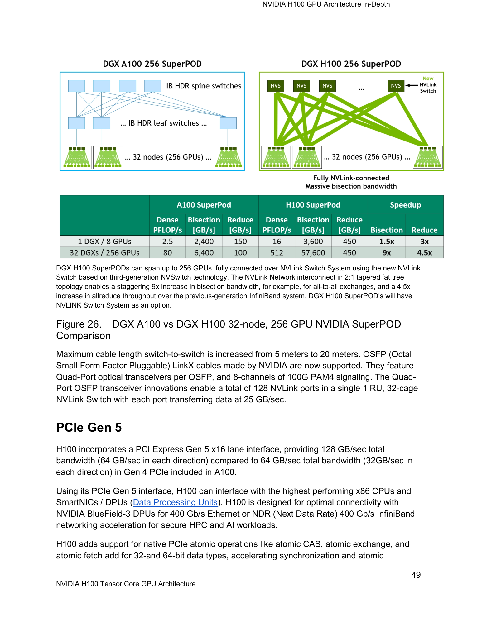
解读: DGX A100 vs DGX H100 32-node/256-GPU SuperPOD对比。H100 SuperPOD通过NVLink Switch System将256个GPU连接在统一NVLink域——这是革命性变化。A100 SuperPOD跨节点必须走InfiniBand(200 Gbps),NVLink仅限节点内8 GPU。H100 SuperPOD中256 GPU可通过NVLink Switch实现全NVLink带宽跨节点通信(每GPU 900 GB/s)。SuperPOD FP8算力: 256 × 1,978.9 = ~507 PFLOPS = 0.5 ExaFLOP FP8 (1 ExaFLOP sparse)。
NVLink Switch System (全新):
- 外部NVLink Switch机箱,基于3rd-gen NVSwitch芯片
- OSFP LinkX光缆连接(最长20m)
- 最大NVLink域: 256 GPU (32 DGX H100 nodes)
- 拓扑: 2:1 tapered fat tree
- 全系统all-to-all带宽: 57.6 TB/s
- 意义: 突破"NVLink限于节点内"历史限制。TP(Tensor Parallelism)可从8-GPU扩展到256 GPU跨节点
6c. Scale-Out Interface #
- InfiniBand: DGX H100配备8× ConnectX-7 NDR (400 Gbps each)
- 总节点间带宽: 8 × 400 = 3.2 Tbps = 400 GB/s (2x DGX A100)
- GPUDirect RDMA + Storage延续
- NVIDIA Quantum-2 InfiniBand Switch: 64端口400G NDR
7. Power, Thermal & Efficiency #
| Parameter | Value |
|---|---|
| TDP (SXM5) | 700W |
| TDP (PCIe) | 350W |
| Cooling | Liquid cooling recommended for SXM5 |
| Process | TSMC 4N custom |
7a. 能效代际对比 #
| Metric | A100 SXM4 (400W) | H100 SXM5 (700W) | Improvement |
|---|---|---|---|
| FP16 TC TFLOPS/W | \( 312/400 = 0.780 \) | \( 989.4/700 = 1.413 \) | 1.81x |
| FP8 TC TFLOPS/W | — | \( 1978.9/700 = 2.827 \) | — |
| FP16 Sparse TFLOPS/W | \( 624/400 = 1.560 \) | \( 1978.9/700 = 2.827 \) | 1.81x |
| FP32 CUDA TFLOPS/W | \( 19.5/400 = 0.049 \) | \( 66.9/700 = 0.096 \) | 1.96x |
| FP64 TC TFLOPS/W | \( 19.5/400 = 0.049 \) | \( 66.9/700 = 0.096 \) | 1.96x |
H100能效提升~1.8x(FP16 TC)来自: 4N工艺(~1.5x能效改善) + TC微架构优化(30% operand delivery功耗下降)。TDP增长75%(400→700W)但性能增长217%(312→989.4 TF) → 净能效 \( 1.81\times \)。700W TDP使SXM5液冷几乎必需(DGX H100标配液冷)。
8. Software & ISA Impact #
8a. ISA Changes (Compute Capability 9.0) #
新增指令:
- WGMMA指令族:
wgmma.mma_async.sync.aligned.m64nNkK.{f16,e4m3,e5m2,tf32,f64}— 4-warp协作MMA,可从SMEM直接读operand(bypass RF) - TMA指令:
cp.async.bulk.tensor.{1-5}d.shared::cluster.global— Global→Shared tensor搬运;cp.async.bulk.tensor.{1-5}d.global.shared::cta— Shared→Global - DSMEM指令:
ld.shared::cluster/st.shared::cluster— 跨SM shared memory访问 - Cluster Barrier:
barrier.cluster.arrive/wait— Cluster级同步 - Transaction Barrier:
mbarrier.arrive.expect_tx— 带byte count的异步事务barrier - DPX:
vimnmx— 动态规划fused compare-select-accumulate - FP8 Convert:
cvt.rn.f8.f16/cvt.rn.f16.f8— FP8↔FP16精度转换 - Setmaxnreg: 动态调整warp可用寄存器数
Figure 5: TMA Architecture #
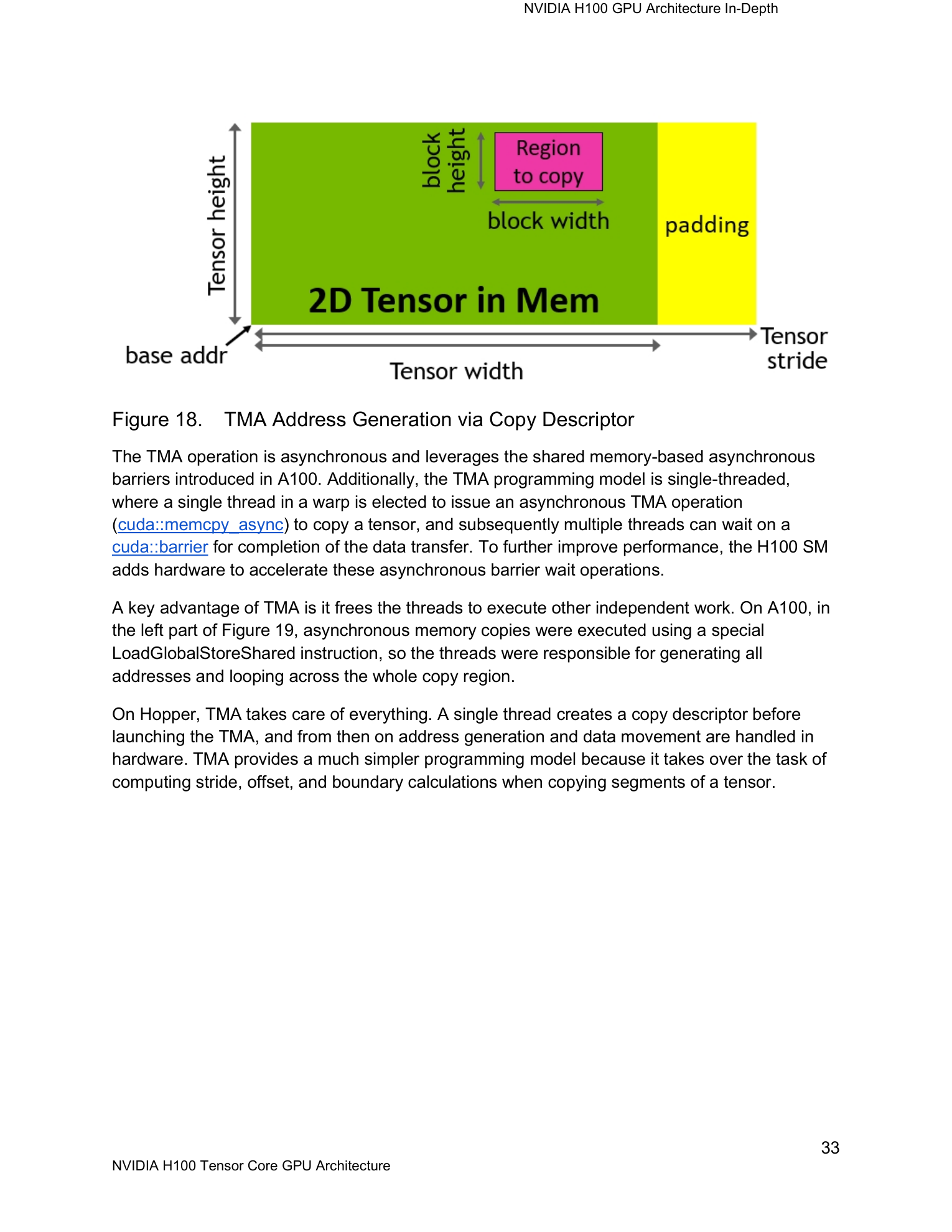
解读: TMA工作原理。TMA Copy Descriptor包含tensor的base address、shape、stride、padding信息(设置一次)。TMA指令接收descriptor + coordinate(tile起始坐标)→硬件自动计算所有元素物理地址→批量异步搬运到Shared Memory。与A100的LDGSTS(每线程独立计算地址+逐向量拷贝)对比,TMA一次搬整个multi-dimensional tile(1D-5D)且硬件处理boundary padding(越界填零)。TMA还支持Shared→Global(store_async)和Cluster内DSMEM间搬运。
Figure 6: Thread Block Clusters #
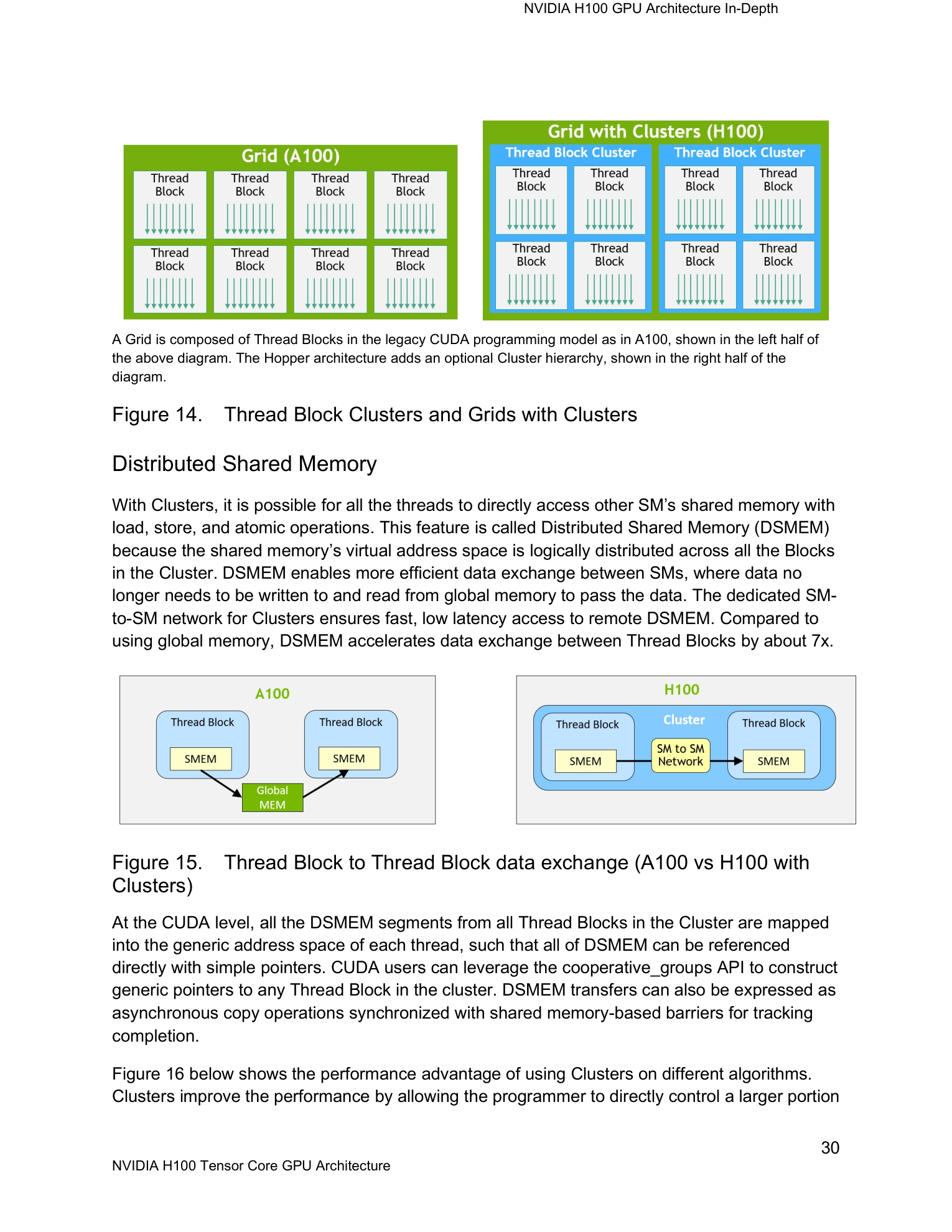
解读: Thread Block Cluster编程模型。左: 传统CUDA(A100) Grid包含独立Thread Blocks,跨Block通信只能通过Global Memory/L2。右: H100 Grid可包含Clusters,每Cluster内多Block调度在相邻SM上,通过DSMEM直接通信(bypass L2)。图中展示Cluster内Block间数据交换路径——通过SM间专用网络(GPC内)而非L2 crossbar。对split-K GEMM至关重要: 不同Block计算同一output tile的部分结果,通过DSMEM直接累加。
8b. 编译器与软件栈 #
- CUDA 12.0+: 支持Compute Capability 9.0
- CUTLASS 3.x: 全面重写,原生支持WGMMA + TMA + Cluster
- transformer_engine: NVIDIA FP8训练专用库,集成PyTorch/JAX
- TensorRT-LLM: 自动利用H100 FP8推理路径
- NCCL: 利用NVSwitch in-network AllReduce加速集合通信
Figure 7: Transformer Engine Conceptual Operation #
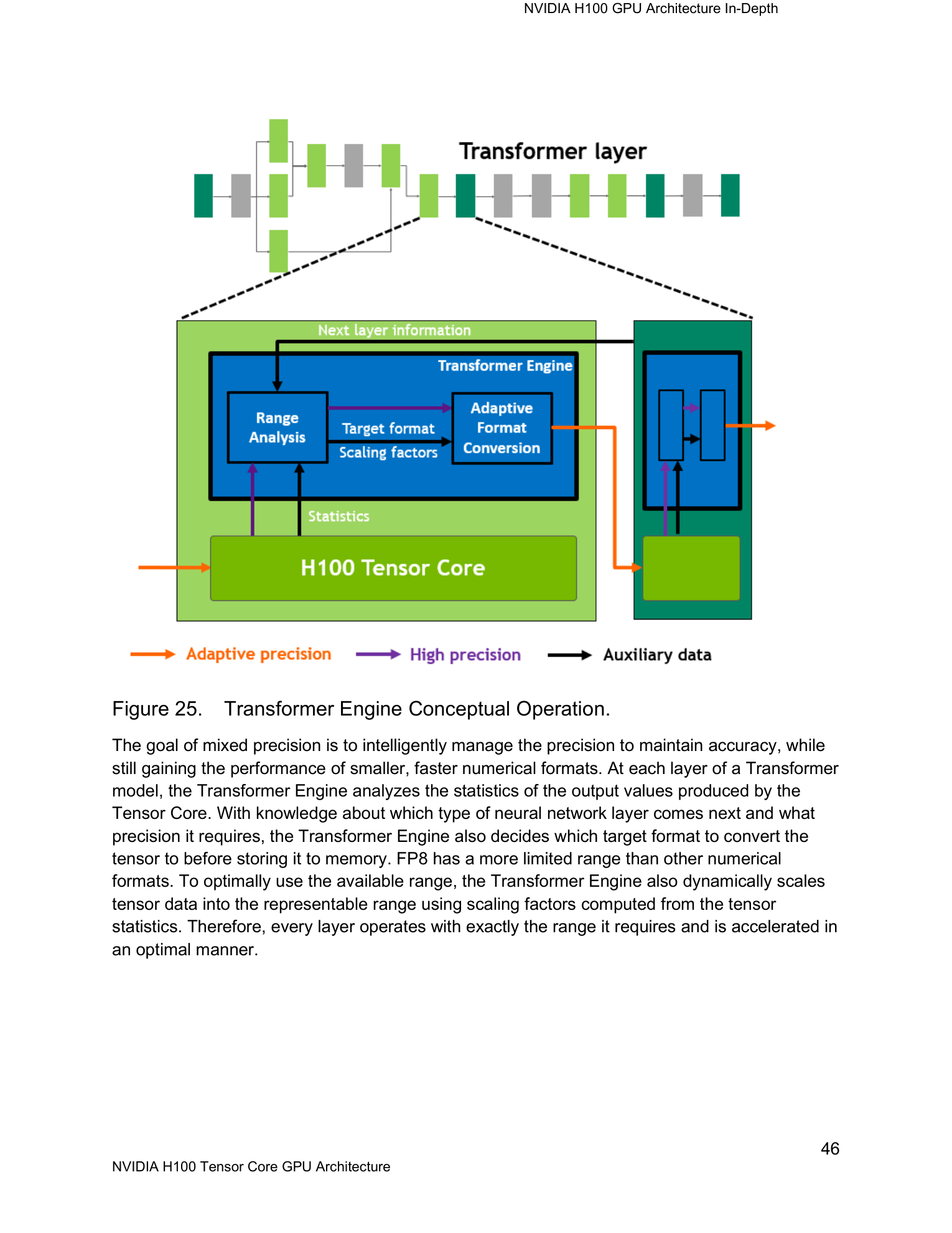
解读: Transformer Engine工作流程。每层Transformer的Linear/Attention中: (1) 输入FP16/BF16经量化→FP8(E4M3 for forward, E5M2 for backward),使用per-tensor FP32 scaling factor; (2) FP8 Tensor Core执行矩阵运算,FP32累加器保持精度; (3) 输出反量化回FP16/BF16。Delayed scaling策略: 基于前几iteration的amax统计量预测当前最优scale。Master weights和optimizer states始终FP32。
8c. 编程模型变化 #
- Warp size: 32 (unchanged)
- Max threads per block: 1,024 (unchanged)
- Max shared memory per block: 227 KB (from A100's 163 KB, +39%)
- Max registers per thread: 255 (unchanged)
- 新增: Thread Block Cluster (max 16 blocks/cluster)
- 新增: TMA descriptor-based tensor搬运 (替代per-thread async copy)
- 新增: WGMMA warp-group协作MMA (4 warps = 128 threads)
- 异步pipeline进化: A100的3-stage async copy → H100的TMA + Transaction Barrier全异步pipeline
9. AI Workload Impact Analysis #
9a. GEMM (矩阵乘法) #
- 理论峰值提升: 3.2x FP16 TC, 6.3x FP8 TC vs A100
- 实际大GEMM: FP16 ~2.8-3.0x; FP8 ~5-6x (Transformer Engine overhead轻微)
- Compute-bound阈值提高: A100 n≥512 → H100 n≥1024 (Ops:Byte翻倍)
- WGMMA+TMA效果: CUTLASS 3.x kernel TC utilization从A100~70% → H100~85-90%
9b. Attention #
- Flash Attention on H100: TMA直接搬运Q/K/V tile, DSMEM允许cross-SM partial softmax reduction → 效率远高于A100
- KV Cache: 80GB HBM3限制与A100相同(H200的141GB缓解)
- 长序列: 256KB SMEM缓存更大Q/K tile → 减少HBM读取
9c. MoE (Mixture of Experts) #
- NVLink Switch System: EP可跨节点扩展(256 GPU NVLink域)——MoE训练重大突破
- All-to-All: 900 GB/s NVLink + in-network reduction → expert token routing延迟大幅降低
- FP8 Expert Weights: 每expert显存占用减半 → 同等80GB可容纳2x更多expert参数
9d. Training vs Inference #
- 训练: Transformer Engine(FP8自动) + WGMMA(高TC util) + TMA(data staging加速) + NVLink Switch(256-GPU TP/EP) → LLM训练claimed 30x加速
- 推理: FP8 TC(1978.9 TFLOPS) + Flash Attention + MIG(7实例+Secure MIG) → 高吞吐低延迟
- 分化: Transformer Engine面向训练(需per-tensor scaling基础设施);推理倾向直接FP8-PTQ
10. Competitive Positioning — H100 vs AMD MI250X / MI300X #
| Metric | H100 SXM5 (2022) | MI250X (2021) | MI300X (2023) |
|---|---|---|---|
| Process | TSMC 4N | TSMC N6 | TSMC N5/N6 |
| Die/Package | 814 mm² (mono) | 2× 228 mm² (MCM) | 8 XCDs + 4 IODs (chiplet) |
| Transistors | 80B | 58B | 153B |
| CUs/SMs | 132 SMs | 220 CUs | 304 CUs |
| FP16 Matrix | 989.4 TFLOPS | 383 TFLOPS | 1,307.4 TFLOPS |
| FP8 Matrix | 1,978.9 TFLOPS | — | 2,614.9 TFLOPS |
| FP64 Matrix | 66.9 TFLOPS | 95.7 TFLOPS | 163.4 TFLOPS |
| Memory | 80 GB HBM3 | 128 GB HBM2e | 192 GB HBM3 |
| Bandwidth | 3.35 TB/s | 3.28 TB/s | 5.3 TB/s |
| Interconnect | NVLink 900 GB/s | IF 800 GB/s | IF 896 GB/s |
| TDP | 700W | 500W | 750W |
| Sparsity | 2:4 Structured | No | No |
| Transformer Engine | Yes (FP8 auto) | No | No |
| TMA / DSMEM | Yes | No | No |
| SW Ecosystem | CUDA (dominant) | ROCm | ROCm (maturing) |
竞品分析:
- vs MI250X: H100在所有AI metrics碾压(FP16 2.6x)。MI250X唯一优势是FP64(95.7 vs 66.9 TF, 1.43x)和显存(128 vs 80 GB)。MI250X是A100的竞品而非H100的。
- vs MI300X: MI300X通过chiplet(8 XCD)在spec全面超越——FP16 1.32x, FP8 1.32x, FP64 2.44x, Memory 2.4x(192 vs 80 GB), BW 1.58x。192GB显存是杀手级优势: Llama-2 70B FP16可单卡(需140GB),H100需2卡。
- H100护城河: (1) CUDA生态——cuBLAS/cuDNN/TensorRT/Flash Attention优化深度远超ROCm; (2) Transformer Engine——FP8自动混合精度无对等方案; (3) NVLink Switch——256 GPU NVLink域对超大规模训练独有优势; (4) TMA/DSMEM——硬件数据搬运加速的结构性效率优势; (5) 2:4 Sparsity——MI300X无此硬件,H100 FP8 sparse(3,957.8 TF)反超MI300X dense(2,614.9 TF)达51%
- MI300X优势: 显存容量(2.4x)和HBM带宽(1.58x)——对memory-bound LLM推理(长序列、大batch KV Cache)是决定性优势
11. Comprehensive Spec Sheet #
| Category | Parameter | H100 SXM5 |
|---|---|---|
| Architecture | Architecture Name | NVIDIA Hopper |
| GPU Code Name | GH100 | |
| Process Node | TSMC 4N (custom) | |
| Die Size | 814 mm² | |
| Transistors | 80 billion | |
| Packaging | Monolithic die | |
| Compute | GPCs | 8 |
| TPCs | 66 | |
| SMs | 132 | |
| CUDA Cores (FP32) | 16,896 (128/SM) | |
| FP64 Units | 8,448 (64/SM) | |
| Tensor Cores | 528 (4/SM, 4th gen) | |
| TC Boost Clock | 1,830 MHz | |
| CUDA Max Boost | ~1,980 MHz | |
| TC Performance | FP8 TC | 1,978.9 TFLOPS (3,957.8 sparse) |
| FP16 TC | 989.4 TFLOPS (1,978.9 sparse) | |
| BF16 TC | 989.4 TFLOPS (1,978.9 sparse) | |
| TF32 TC | 494.7 TFLOPS (989.4 sparse) | |
| FP64 TC | 66.9 TFLOPS | |
| INT8 TC | 1,978.9 TOPS (3,957.8 sparse) | |
| CUDA Performance | FP64 | 33.5 TFLOPS |
| FP32 | 66.9 TFLOPS | |
| FP16 | 133.8 TFLOPS | |
| BF16 | 133.8 TFLOPS | |
| Memory | HBM Type | HBM3 |
| Capacity | 80 GB | |
| Stacks | 5 | |
| Controllers | 10 × 512-bit | |
| Bandwidth | 3,350 GB/s | |
| L2 Cache | 50 MB | |
| L1/SMEM per SM | 256 KB (max 228 KB SMEM) | |
| Register File per SM | 256 KB | |
| Interconnect | NVLink Version | 4.0 |
| NVLink Links | 18 | |
| NVLink BW (bidir) | 900 GB/s | |
| NVLink Domain (Switch) | 256 GPU | |
| NVSwitch | v3 (64 ports, 3.2 TB/s) | |
| PCIe | Gen 5 x16 (128 GB/s) | |
| Power | TDP (SXM5) | 700W |
| TDP (PCIe) | 350W | |
| FP16 TC TFLOPS/W | 1.413 | |
| FP8 TC TFLOPS/W | 2.827 | |
| Features | Transformer Engine | Yes (FP8/FP16 auto) |
| TMA | Yes (1D-5D tensor) | |
| Thread Block Clusters | Yes | |
| Distributed Shared Memory | Yes | |
| MIG | Up to 7 Instances + Secure MIG | |
| Sparsity | 2:4 Structured | |
| DPX Instructions | Yes | |
| Compute Capability | 9.0 |
12. Infrastructure Impact #
| Layer | Impact |
|---|---|
| Algorithm | FP8 Transformer Engine改变训练精度策略——从"手动AMP FP16/BF16"到"自动FP8/FP16切换";per-tensor delayed scaling成为数值精度新研究方向;催生FP8-aware量化训练算法和MXFP8标准研究 |
| Kernel | TMA彻底改变data staging范式: 从"warp threads计算地址+load+store"到"单指令DMA搬运整tile";WGMMA从SMEM直接读operand(bypass RF)→减少RF bandwidth pressure;Cluster+DSMEM使跨SM reduction成为可能(Flash Attention v3, split-K GEMM)。CUTLASS 3.x全面重写以利用新ISA |
| Framework | transformer_engine库成为PyTorch/JAX的FP8训练标准接口;TensorRT-LLM利用FP8路径优化LLM推理;DeepSpeed/Megatron适配Transformer Engine;PyTorch 2.0+通过torch.float8_e4m3fn原生支持FP8 dtype |
| LLM | FP8使LLM训练compute降2x(vs FP16)→GPT-3级模型训练时间减半;80GB显存仍是瓶颈(Llama-70B FP16需140GB→2卡)→催生H200(141GB);NVLink Switch使TP可跨节点→更大模型并行策略更灵活 |
| Agent | FP8推理(1978.9 TFLOPS)+Flash Attention→实时推理延迟大幅降低;Secure MIG允许多推理agent安全共享GPU;vLLM/TensorRT-LLM的PagedAttention+FP8 kernel首先在H100达生产级 |
| Cluster | DGX H100+NVLink Switch System定义新一代AI超算: 256-GPU NVLink域→节点间TP/EP成为可能;单SuperPOD达0.5 ExaFLOP FP8;NVSwitch 3.0 in-network AllReduce减少SM参与collective开销;700W TDP推动数据中心液冷标准化 |